
Xiao Kui Li
China Coal Technology Engineering Group Chongqing Research Institute, Chongqing, 400700, China
Journal of Applied Sciences
Year: 2014 | Volume: 14 | Issue: 15 | Page No.: 1720-1727


ABSTRACT
In order to expand the application of synchronous rectification, the technology using ZVS synchronous rectifier is studied which is based on the IPT resonant converter. By using its own resonant characteristic, a novel control method that AC-DC section of the resonant converter works in ZVS SR state is proposed in this study. First of all, the ZVS working operation of SR is analyzed and equivalent circuits for each operation mode are also given. On that basis, the novel control method is proposed. Then, according to the differential equations of equivalent circuit, the state space model is established. In order to make full-bridge SR network of the secondary circuit work in ZVS state, the ZVS operating point can be obtained by solving the fixed point function which is based on the state space model and stroboscopic mapping method. Moreover, operating principle of control circuit for ZVS SR is also presented. Finally, experimental results verify the effectiveness of control method proposed in this study.
PDF Abstract XML References Citation
Received: November 26, 2013;
Accepted: February 18, 2014;
Published: April 18, 2014
How to cite this article
Xiao Kui Li, 2014. Research ZVS Synchronous Rectification of Resonant Converter. Journal of Applied Sciences, 14: 1720-1727.
DOI: 10.3923/jas.2014.1720.1727
URL: https://scialert.net/abstract/?doi=jas.2014.1720.1727
DOI: 10.3923/jas.2014.1720.1727
URL: https://scialert.net/abstract/?doi=jas.2014.1720.1727
INTRODUCTION
Synchronous Rectifier (SR) has been widely adopted in the low output voltage applications to reduce the conduction loss of the output rectifier (Lim et al., 2010). Therefore, SR has become a research hotspot associated with the AC-DC converter of all kinds of switching power supply.
At present, researches on synchronous rectification are mainly concentrated in buck converter (Stankovic et al., 2012), forward converter (Coban and Cadirci, 2011), flyback converter (Kim et al., 2014), half-bridge converter (Jeong, 2008), push-pull converter. However, the application of SR in a resonant converter has been rarely studied.
Analyzing the existing synchronous rectifier converters, theirs rectifier section generally work in hard switching state. Therefore, when the switching frequency of SR is high, large switching losses are caused and the system efficiency is reduced. At the same time, it is easy to influence the main circuit operation of converter and reduce the system performance because synchronous rectification of the existing converters usually is adopted self-driving mode.
However, compared with other converters, resonant converter has the advantages of small volume, high transmission efficiency. In particular, capacitor voltage and inductor current in the resonant tank are sine wave, so that a wide range of switching network worked in Zero Voltage Switching (ZVS) or Zero Current Switching (ZCS) can be easy to achieve. Further analysis shows that, due to the existence of resonant tank, the traditional self-driving cannot be adopted to achieve the SR output for resonant converter.
In this study, the resonant converter circuit based on Inductive Power Transfer (IPT) (Li et al., 2012) is as a research object. By using its own resonant characteristic, a novel control method that AC-DC section of the resonant converter works in ZVS SR state is proposed.
This study is organized as follows. ZVS operation principle of SR for the IPT resonant converter is presented. Then, the state space model of the resonant converter is established. In order to quickly and accurately calculate the ZVS-operating cycle of SR, the fixed point function about it is established by using a stroboscopic mapping method which is based on the state space model. Moreover, operating principle of control circuit for ZVS SR is also presented. Finally, experimental results are conducted to verify that control method proposed in this study is effective for the resonant converter circuit based on IPT.
ZVS OPERATION PRINCIPIE OF SR
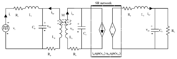
In this study, the IPT resonant converter circuit used synchronous rectifier is showed in Fig. 1 which consists of a primary and a secondary circuit. In the primary circuit, the switching network (S1, S4and S2, S3) convert the dc voltage source Edc to high frequency ac that drives an LCL resonant tank consisting of Li, CP and LP. Therefore, a high-frequency ac can be generated in the primary coil LP.
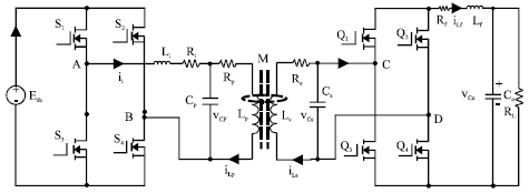 | |
| Fig. 1: | Circuit diagram of the IPT resonant converter used SR |
Due to the magnetic field coupling, a high-frequency ac voltage is induced in the secondary coil Ls which is then completely tuned by the parallel capacitor Cs. In the secondary circuit, the two switching pairs (Q1, Q4 and Q2, Q3) constitute a full-bridge SR network. Lf and Co constitute a filter link, RL is the load resistance and M is the mutual inductance coupling value between primary coil and secondary.
In order to simplify the analysis, following assumptions are made for the analyses of operating modes:
| • | All MOSFETs are considered to be ideal |
| • | The input voltage source Edc is ideal |
| • | The filter inductor Lf current is continuous |
Critical operation waveforms of the system are given in Fig. 2, for steady-state operation. vAB is the input voltage of the primary full-bridge converter. ii is the flowing current of inductor Li. vCs is the voltage across capacitor Cs. vQi(i = 1, 2, 3, 4) is the drain-source voltage of switch Qi in the secondary SR network. Gi(i = 1, 2, 3, 4) is the drive voltage of switch Qi in the secondary SR network.
Meanwhile, so as to clearly analyze operation modes of the circuit shown in Fig. 1, time t0 is assumed to be the starting point of one operational cycle and stipulate positive direction of the dc energy Edc injected is that switches S1 and S4 are turned on. When Switches Q1 and Q4 are turned on, this is SR output positive direction of the AC voltage vCs. So, effective circuits for each mode in one operational cycle are given in Fig. 3.
Mode 1 (t0-t1): The state of primary circuit is that dc energy is injected from negative direction. Switches S2 and S3 are turned on when S1 and S4 are turned off. The state of secondary circuit is that the AC voltage vCs is output from positive direction of the synchronous rectifier.
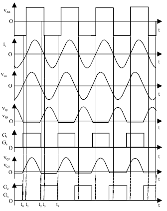 | |
| Fig. 2: | Critical steady-state operation waveforms |
Switches Q1 and Q4 are reversely turned on when Q2 and Q3 are turned off. In this mode, its equivalent circuit is shown in Fig. 3a.
Mode 2 (t1-t2): The state of primary circuit is that energy is injected from positive direction. Switches S1 and S4 are turned on when S2 and S3 are turned off. The state of secondary circuit is that the AC voltage vCs is output from positive direction of the synchronous rectifier. Switches Q1 and Q4 are reversely turned on when Q2 and Q3 are turned off. In this mode, its equivalent circuit is shown in Fig. 3b.
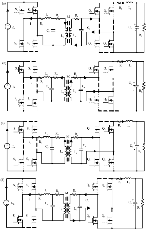 | |
| Fig. 3(a-d): | Equivalent circuits for each operation mode (a) Mode 1, (b) Mode 2, (c) Mode 3 and (d) Mode 4 |
Mode 3 (t2-t3): The state of primary circuit is that energy is injected from positive direction. Switches S1 and S4 are turned on when S2 and S3 are turned off. The state of secondary circuit is that the AC voltage vCs is output from negative direction of the synchronous rectifier. Switches Q2 and Q3 are reversely turned on when Q1 and Q4 are turned off. In this mode, its equivalent circuit is shown in Fig. 3c.
Mode 4 (t3-t4): The state of primary circuit is that energy is injected from negative direction. Switches S2 and S3 are turned on when S1 and S4 are turned off. The state of secondary circuit is that the AC voltage vCs is output from negative direction of the synchronous rectifier. Switches Q2 and Q3 are reversely turned on when Q1 and Q4 are turned off. In this mode, its equivalent circuit is shown in Fig. 3d.
Through the above analysis, the switching states of two primary switching pairs (S1, S4 and S2, S3) are changed, when the current of inductance Li is zero. This time that their switching states are changed between turned on and off, the current flowing through them are zero.Hence, the primary switching inverter works in zero current soft switching state.
In the secondary circuit, the voltage vCs of the capacitor Cs is a sinusoidal voltage. It is obvious to know that when vCs is equal to zero, the drain to source voltage vQi of the four switches (Q1, Q2, Q3 and Q4) are also equal to zero. Therefore, ZVS SR output of the AC voltage vCs can be achieved by controlling the switching pairs (Q1, Q4 and Q2, Q3) turned on or off when vCs is equal to zero.
In summary, the primary full-bridge converter working in zero current soft switching state and the secondary full-bridge SR network working in zero voltage soft switching state can be achieved in the IPT resonant converter.
STEADY STATE MODELING
In order to carry out the numerical analysis of the circuit shown in Fig. 1, a steady state mathematical model of the system is necessary to be established.
Assume that the switching period of the primary full-bridge inverter shown in Fig. 1 is T under steady-state conditions. Then the input voltage of the primary resonant tank can be described as:
| (1) |
| (2) |
where, m is zero or a positive integer.
In the secondary circuit shown in Fig. 1, switch transitions of the full-bridge SR network are determined by the polarity change of the resonant voltage vCs. Consequently, a sign function Sgn(vCs) can be used to represent operation of the full-bridge SR network:
![]()
After such that representations, the circuit diagram shown in Fig. 1 is simplified as an equivalent circuit shown in Fig. 4.
According to Kirchhoff’s current and voltage laws, the differential equations of the equivalent circuit as shown in Fig. 4, can be presented as follows:
| (3) |
| (4) |
| (5) |
| (6) |
| (7) |
| (8) |
| (9) |
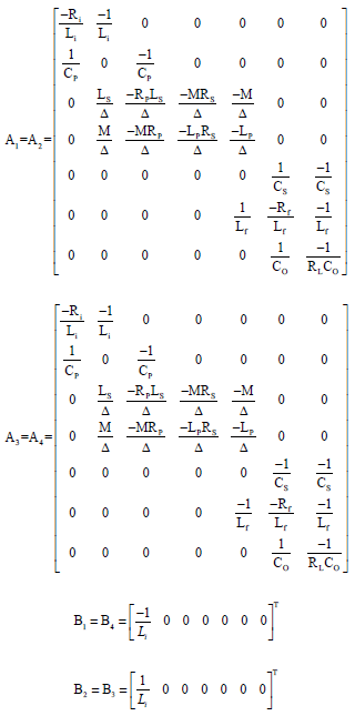
where, Δ = LSLP-M2. By choosing x = [ii vCp iLp iLs vCs iLf vCo]T and u = [Edc] as the state vector and the input vector of the system, respectively. According to the differential Eq. 3-9, the system can be described by the following state space model:
| (10) |
where, i represent the figures of operation modes shown in Fig. 3:
 | |
| Fig. 4: | Equivalent circuit of the IPT resonant converter used SR |
DETERMING ZVS-OPERATING CYCLE OF SR
The ZVS operating point of the SR circuit must be obtained to make full-bridge SR network of the secondary circuit work at zero voltage soft switching state.
The system matrix A1, A2, A3, A4 are invertible, so that the analytical solution of Eq. 1) has the following format:
| (11) |
where, x0 = x(t)|t = 0 and φ(t) = eAtx(t).
As can be seen from Fig. 2 and 3, during one operational cycle, the final value of each mode equals to the initial value of the next mode. Therefore Eq. 11 can be extended into four stroboscopic mapping equations to cover all the four modes (Liu et al., 2011):
| (12) |
| (13) |
| (14) |
| (15) |
where, I is a 7-order unit matrix and x0 is the initial value of the circuit state vector.
Under steady-state conditions, the state vector repeats periodically which means the state vector results in a fixed point x* is described as follows:
| (16) |
Substitute Eq. 13-15 into 12, the fixed point x* can be expressed as follows:
| (17) |
where, α = (I-φ4φ3φ2φ1)-1.
Corresponding to the ZVS condition of the full-bridge SR network, the voltage vCs must be zero at the switching instants. Then from Eq. 17, ZVS operation cycle (TZVS) of the full-bridge SR network can be obtained as follows (Tang et al., 2009; Sun et al., 2011):
| (18) |
where, Y = [0 0 0 0 1 0 0] is a selection matrix for the state variable vCs.
OPERATING PRINCIPIE OF CONTROL CIRCUIT
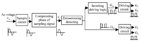
In order to achieve zero voltage soft switching state operation of the secondary full-bridge SR network, the working operation of control circuit as shown in Fig. 5.
The operation processes of the control circuit are described as follows. First of all, the AC voltage vCs through the sampling circuit, a weak signal (v1) with the same frequency can be obtained. The phase of the signal (v1) must be compensated, because the control circuit operation can lead to a delay of the signal. To precisely control switching pairs (Q1, Q4 and Q2, Q3) turned on or off, the zero-crossing detection circuit is designed for detecting of the AC voltage vCs. Therefore, after the previous circuit, the digital signal (Gin2) digital signal can be obtained. Gin2 is used as the input of driving circuit for switches (Q2, Q4). In order to achieve the two SR switching pairs (Q1, Q4 and Q2, Q3) working in zero voltage soft switching state, the two drive voltage pairs (G1, G4 and G2, G3) must be complementary.
 | |
| Fig. 5: | ZVS control diagram of the full-bridge SR inverter |
So, invert Gin2 and then Gin1 is used as the input of driving circuit for switches (Q1, Q3).
EXPERIMENTAL STUDY
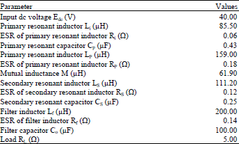
According to the Fig. 1 and operating principle of control circuit. The experimental circuit is built to validate the feasibility of control method proposed and the experimental parameters are shown in Table 1.
According to Eq. 18, the parameters shown in Table 1 are substituted into it. Therefore, the ZVS operation cycle (TZVS) of the full-bridge SR network can be obtained by solving M file in matlab. By solving Eq. 18, TZVS is equal to 13.21 μsec. It means that the frequency of the driving voltage (G1, G2, G3 and G4) is 75.7 kHz.
According to the result of TZVS, MOSFET IRFB4110 is selected as the component for SR and control circuit of the experiment for SR is well designed.
The experimental waveforms of the input voltage (vAB) of the primary full-bridge converter and the flowing current (ii) of inductor Li are showed in Fig. 6. From Fig. 6, it can be seen that the polarity of voltage (vAB) is changed when the current ii is equal to zero. Hence, the conclusion that the two primary switching pairs (S1, S4 and S2, S3) works at zero current soft switching state can be clearly obtained.
Figure 7 shows the experimental waveforms of the waveforms of vCs, G1 and G2. From Fig. 7, it can be seen that the voltage vCs is a sine wave. Meanwhile, when vCs is greater than zero, switch Q1 is turned on owing to G1 driving but switch Q2 is turned on owing to G2 driving when vCs is less than than zero.
The experimental waveforms of vCs, vQ1, vQ4, G1 and G4 are shown in Fig. 8. From Fig. 8, it can be seen that switches Q1, Q4 are simultaneously turned on or off because of the drive voltage G1, G4, respectively. At same time, it also can be found that the switching states of Q1 and Q4 are changed when the drain to source voltage of Q1 and Q4 is equal to zero.
Figure 9 shows the experimental waveforms of the drive voltage G2, G3, the AC voltage vCs and the drain to source voltage of Q2, Q3.
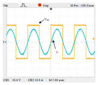 | |
| Fig. 6: | Experimental waveforms of the current ii and voltage vAB |
| Table 1: | Experimental parameters |
 | |
As it can be seen from Fig. 9, the drive voltage G2, G3 simultaneously drive switches Q2, Q3 which are turned on or off, respectively. Moreover, it can be found that the switching states of Q2 and Q3 are changed when the drain to source voltage of Q2 and Q3is equal to zero.
Analyzing the Fig. 7-9, it can be seen that when vCs is in the positive half cycle, switches Q1, Q4 are turned on and switches Q2, Q3 are turned off.
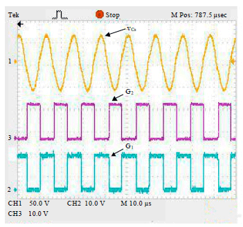 | |
| Fig. 7: | Experimental waveforms of vCs, G1 and G2 |
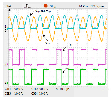 | |
| Fig. 8: | Experimental waveforms of vCs, vQ1, vQ4,G1 and G4 |
When vCs is in the negative half cycle, switches Q2, Q3 are turned on and switches Q1, Q4 are turned off. This means that the AC voltage vCs has been synchronously rectified. Moreover, all of the drain to source voltage of four switches Q1, Q2, Q3 and Q4 are equal to zero when switching states of four switches are changed. This means that the secondary full-bridge SR network works in zero voltage soft switching state.
Therefore, the experimental results show that zero current soft switching state of the primary full-bridge and zero voltage soft switching state of the secondary full-bridge SR network have been achieved in the IPT resonant converter.
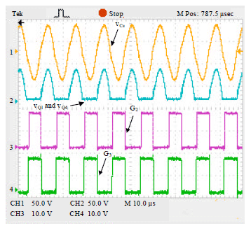 | |
| Fig. 9: | Experimental waveforms of vCs, vQ2, vQ3, G2 and G3 |
CONCLUSION
In this study, due to resonance characteristics of the resonant converter based on IPT, a novel control method has been proposed to achieve ZVS SR state operation for the AC-DC network of the resonant converter. A steady state mathematical model has been established to determine the ZVS operating point of SR network which is based on the analysis about ZVS operation principle of SR and stroboscopic mapping method. The control circuit working operation has also been presented to guide the design of corresponding hardware circuit. Finally, the method proposed in this study has been verified by experimental results.
REFERENCES
- Lim, C.Y., Y.C. Liang and G.S. Samudra and N. Balasubramanian, 2010. A smart-power synchronous rectifier by CMOS process. IEEE Trans. Power Electron., 25: 2469-2477.
CrossRef - Stankovic, A.V., L. Nerone and P. Kulkarni, 2012. Modified synchronous-buck converter for a dimmable HID electronic ballast. IEEE Trans. Ind. Electron., 59: 1815-1824.
CrossRef - Coban, A. and I. Cadirci, 2011. Active clamped two-switch forward converter with a soft switched synchronous rectifier. IET Power Electron., 4: 908-918.
CrossRef - Kim, K.T., J.M. Kwon, H.M. Lee and B.H. Kwon, 2014. Single-stage high-power factor half-bridge flyback converter with synchronous rectifier. IET Power Electron., 7: 1-10.
CrossRef - Jeong, G.Y., 2008. High efficiency asymmetrical half-bridge converter using a self-driven synchronous rectifier. IET Power Electron., 1: 62-71.
CrossRef - Li, H.L., A.P. Hu and G.A. Covic, 2012. A direct AC-AC converter for inductive power-transfer systems. IEEE Trans. Power Electron., 27: 661-668.
CrossRef - Liu, C., A.P. Hu and N.K. Nair, 2011. Modelling and analysis of a capacitively coupled contactless power transfer system. IET Power Electron., 4: 808-815.
CrossRef - Tang, C.S., Y. Sun, Y.G. Su, S.K. Nguang and A.P. Hu, 2009. Determining multiple Steady-state ZCS operating points of a Switch-mode contactless power transfer system. IEEE Trans. Power Electron., 24: 416-425.
CrossRef - Sun, Y., C. Tang, A.P. Hu, H.L. Li and S.K. Nguang, 2011. Multiple soft-switching operating points-based power flow control of contactless power transfer systems. IET Power Electron., 4: 725-731.
CrossRef