
Shihan Sajeed
27/8 K.M. Das Lane, Tikatully, Dhaka-12.3, Bangladesh
Nigar Sultana
27/8 K.M. Das Lane, Tikatully, Dhaka-12.3, Bangladesh
Research Journal of Physics
Year: 2012 | Volume: 6 | Issue: 1 | Page No.: 19-30


ABSTRACT
Transverse modes of electromagnetic fields are proposed to be encoded as qubits for simulating quantum computation. The method relies on simple optical devices such as Mach-Zehnder Interferometer (MZI) and phase shifter built on 2-transverse-mode-waveguides. The possibility of this encoding scheme was designed, simulated and verified through rigorous numerical analyses using the Beam propagation method. The proposed logic gates have the potential of being more compact and easily realizable than some other optical implementation proposals since it is based on planar light wave circuit technology.
PDF Abstract XML References Citation
Received: November 03, 2011;
Accepted: March 17, 2012;
Published: June 20, 2012
How to cite this article
Shihan Sajeed and Nigar Sultana, 2012. Simulation of NOT and sqrt (NOT) Logic for 2-transverse-mode-waveguide Qubits. Research Journal of Physics, 6: 19-30.
URL: https://scialert.net/abstract/?doi=rjp.2012.19.30
URL: https://scialert.net/abstract/?doi=rjp.2012.19.30
INTRODUCTION
Recently, there has been great interest in using optical devices as ultrafast logic devices for signal processing, communication and computations (Pramono and Endarko, 2001; Wu et al., 2007). Some studies about the optical waveguide structures and devices made from linear and nonlinear materials have been proposed by Wu et al. (2008) and Wu (2004). There has also been great interest in the use of Mach-Zehnder waveguide interferometer for the use of modulation, switching and logic gates, etc. (Liu et al., 2000; Sajeed and Haider, 2010). Optical systems also offer realistic proposal for quantum information processing, long-distance quantum communication and underlie experimental implementations of quantum cryptography. The main obstacle to scalable optical QIP is the need for nonlinear couplings between optical modes at sufficient strength which was theoretically possible but is very difficult to achieve in practice (Turchette et al., 1995). As a result, other proposals (Cerf et al., 1998; Howell and Yeazell, 2000) for using linear optics to benchmark quantum algorithms require exponentially large physical resources.
In this study, we propose a scheme capable of simulating the operations inherent in quantum computing. To represent ‘the qubits’ we chose the ‘Transverse modes of electromagnetic fields’ and simulate the performance of the quantum ‘NOT’ and ![]() gate.
gate.
By properly analyzing the results using the Beam Propagation Method (BPM), it’s been concluded that the proposed scheme can simulate the quantum operations effectively and the proposed realization is more efficient than some of the previous realizations (Salemian and Mohammadnejad, 2008a, b). To our knowledge, this scheme of transforming a pure state into a superposition state using the transverse modes is realized for the first time in literature.
THEORETICAL BACKGROUND
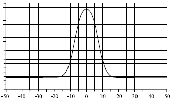
Representation of qubits: Let us consider a dual mode waveguide supporting two modes TE0 and TE1. When the Maxwell’s equations are solved for the guided modes, electric-field profiles are obtained as shown in Fig. 1. The components of the transverse electric fields are solutions of the scalar wave equation (Okamoto, 1999):
| (1) |
The solution Ψ (x, y) of the scalar wave equation and its first derivatives are everywhere continuous and are therefore bounded leading to an Eigenvalue equation for the allowed discrete values of β. The Eigenfunctions constitute a complete set of Eigenfunctions in the sense that an arbitrary solution of the Eq. 1 can be expanded in terms of them. The Eigenfunctions with discrete Eigenvalue are called the normal modes of the waveguide and can be encoded into qubits.
In this study, we considered the TE0 mode as the logical state |0〉 and the other orthogonal normal mode, the TE1 mode as the logical state |1〉 as follows:
| (2) |
| (3) |
If qubits are encoded in this manner its state space will consist of all superposition of the basic normal modes, TE0 and TE1. The encoding scheme is not limited to the TE modes only rather they can be generalized to any other orthogonal modes. We designed the geometry and optical wavelength in such a way that the structure supports only two modes namely TE0 mode and TE1 mode. Thus when they are used to encode qubits they resemble a two state quantum system.
Quantum analysis of a Mach-Zehnder interferometer: Let us consider a dual-mode waveguide MZI as shown in Fig. 2 having a phase shifter φ at one of its arms.
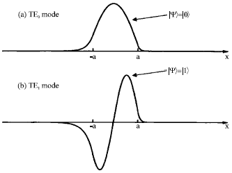 | |
| Fig. 1(a-b): | Electric field profiles for the first two normal modes (a) TE0 (Ψ0) and (b) TE1 (Ψ1) of the three layer structure |
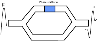 | |
| Fig. 2: | A Mach-Zehnder interferometer consisting of a phase shifter at the upper arm |
The input to the MZI is any one of the two logical inputs |TE0〉 = |0〉 or |TE1〉 = |1〉. At the input side the wave is divided into two and in the absence of the phase shifter at the upper arms, the two waves will undergo equal phase shifts and interfere constructively at the output Y-junction. But due to the presence of the phase shifter, the amount of interference becomes a function of the phase difference ‘φ’. Let the input and the output field be denoted as:
| (4) |
| (5) |
Here, the subscripts of C denote input or output while the superscripts are used to denote the mode number.
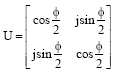
The operator corresponding to the MZI can be represented by the following unitary matrix ‘U’ (Salemian and Mohammadnejad, 2008a, b; Tamir, 1988):
 | (6) |
Selection of phase difference between the two arms: The outputs and inputs are connected by Eq. 4-5 as:
| (7) |
| (8) |
If the MZI is designed such as φ = 0 then output becomes:
| (9) |
| (10) |
In this case, the MZI act as an identity gate. On the contrary, if the MZI is configured such as φ = π, then output can be found by putting φ = π in Eq. 4-5:
| (11) |
| (12) |
Hence, an input TE1 wave will appear at the output as a TE0 mode and vice versa. Thus all logical state |0〉 at the input appear at the output as |1〉 and all logical state |1〉 at the input side appear at the output as state |0〉. As a result the MZI can be efficiently used as a quantum NOT gate.
Again, if φ = π/2, then output becomes:
| (13) |
| (14) |
Hence, a superposition state is produced at the output. The matrix representation of the MZI now becomes:
| (15) |
It resembles the matrix representing the operation of the beam splitter B as:
| (16) |
As a result, the MZI designed for φ = π/2, can effectively be used to performing the ![]() operation.
operation.
DESIGN METHODOLOGY AND SIMULATION
Utilization of the electro-optic effect: In this study, the following parameters were chosen:
| • | Substrate width = 100 μm (x direction) |
| • | Substrate height = 10 μm (y direction) |
| • | Substrate length = 28000 μm (z direction) |
| • | Crystal cut = Z cut |
| • | Propagation direction = Towards z direction |
| • | Substrate material = Diffused LiNbO3 |
| • | Cladding layer height = 2 μm |
| • | Cladding material = air (dielectric) |
| • | Cladding refractive index = 1.00 |
For achieving and control of the required phase shift, electro-optic effect (EO) was utilized. The waveguide material was chosen to be LiNbO3 and the crystal cut and orientation of the LiNbO3 was chosen in such a way that maximum amount of refractive index change could be induced. Thus by placing an electrode material on top and changing the applied voltage on it, required amount of index change and thus the required phase shift can be obtained.
Design of a dual mode waveguide: In order to represent a two state quantum system a dual mode waveguide was designed. Here, the design approach described in (Okamoto, 1999) has been followed. For any wave guide the V-parameter is defined by:
| (17) |
Here, wavelength λ = 1.3 nm:
| • | Substrate R.I, ns = 2.145966 |
| • | Film R.I, nf = 2.148510 |
| • | Cladding R.I, nc = 1 |
The asymmetric measure ‘a’ is:
| (18) |
The required condition for a dual mode guide supporting only 0th and 1st order mode is:
| (19) |
Here:
| (20) |
Thus:
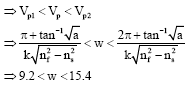 | (21) |
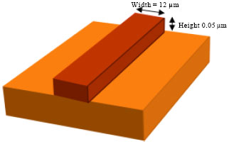
The width of the waveguide was chosen as, w = 12 μm.
Design of the guiding layer
Diffusion parameters: To fabricate a guiding channel Ti in-diffusion process was utilized. The Titanium metal was chosen with parameters:
| • | Titanium height = 0.05 μm |
| • | Titanium width = 12 μm |
| • | Lateral diffusion length DH (μm) = 4 |
| • | Vertical diffusion length DY (μm) = 3.5 |
The metal plate over the substrate is shown in Fig. 3.
The in-diffusion process of titanium inside the LiNbO3 is shown in Fig. 4 and the resultant refractive index distribution is shown in Fig. 5.
 | |
| Fig. 3: | Ti in-diffusion (in extended scale): Ti plate placed over the substrate prior to diffusion |
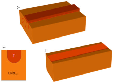 | |
| Fig. 4(a-c): | (a) In-diffusion process of Titanium, (b) The cross sectional view of the diffused material after the in-diffusion process and (c) Top view of the channel/guiding layer created inside the substrate |
 | |
| Fig. 5: | The Refractive index (R.I) distribution inside the guiding layer. The R.I at the center of the guiding layer is 2.220536 and at the LiNbO3 substrate the R.I is 2.220480 |
Selection of parameters for the electrode set: The buffer layer was chosen with the following properties:
| • | Thickness: 0.3 μm |
| • | Horizontal permittivity: 4 |
| • | Vertical permittivity: 4 |
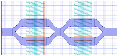
A Snapshot of the layout of the MZI is presented in Fig. 6. In the figure the light blue regions represent the electrode materials deposited over the dielectric.
Figure 5 snapshots of the layout of the MZI with the electrode materials applied.
Calculation of electrode voltage: The relation between electrode voltage and the phase shift is defined as (Nishihara et al., 1989):
| (22) |
In this work:
| • | Distance between the electrodes, d = 6 μm |
| • | Refractive index, n0 = 2.22 |
| • | Electro-optic coefficient, r33 = 30.8 pm/V |
| • | Length of the electrodes, l = 8000 μm |
| • | Operating wavelength, λ = 1.3 μm |
| • | Reduction factor, Γ = 0.3 |
Producing NOT transformation: For achieving Δφ, from (3.15) the voltage was found to be: V = 9.9. During simulation, V = 10 volts was selected to be used.
Producing superposition state: For achieving Δφ = π/2, the voltage was calculated as:
| (23) |
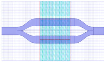 | |
| Fig. 6: | Snapshots of the layout of the MZI with the electrode materials applied |
RESULTS
Simulation of the NOT operation: When a TE0 mode wave was applied at the input of the MZI, the resultant output is shown in Fig. 7. The figure shows the 3-D view of the propagation of optical field (a), the 2-D view of the same field (b) and the transverse field profile at the input (c) and output (d). The same set of results for an input of |1〉 =|TE1〉 is shown in Fig. 8. From Fig. 7 and 8 it was clearly seen that the input TE0 mode wave was converted into a TE1 mode and vice versa and thus effectively reproducing the NOT transformation.
Realization of the ![]() operation: Figure 9 and 10 shows the outputs from the MZI for the logical inputs |0〉 = |TE0〉 and |1〉 = |TE1〉, respectively. The figure shows the 3-D view of the propagation of optical field (a), the 2-D view of the same field (b) the transverse field profile at the input and (c) output (d). The superposition state is clearly visible from the figures.
operation: Figure 9 and 10 shows the outputs from the MZI for the logical inputs |0〉 = |TE0〉 and |1〉 = |TE1〉, respectively. The figure shows the 3-D view of the propagation of optical field (a), the 2-D view of the same field (b) the transverse field profile at the input and (c) output (d). The superposition state is clearly visible from the figures.
In order to prove that the ![]() operation is effectively realized, we connected to such devices back to back as shown in Fig. 11. We recall that:
operation is effectively realized, we connected to such devices back to back as shown in Fig. 11. We recall that:
And:
The resultant outputs for the input state |0〉 and |1〉 are shown in Fig. 12. From Fig. 12 it was clearly seen that the simulated MZI is capable of producing a superposition state from a pure state applied to its input. This scheme of realizing a superposition state is more effective, easily controllable and realizable than some previous proposals (Salemian and Mohammadnejad, 2008a, b).
SCOPE FOR FUTURE WORK
In this study, transverse modes of electro-magnetic fields were considered to be encoded as qubits for simulating the NOT and ![]() transformation. Works based on this encoding technique is presented also by Sajeed et al. (2010) and Salemian and Mohammadnejad (2008b).
transformation. Works based on this encoding technique is presented also by Sajeed et al. (2010) and Salemian and Mohammadnejad (2008b).
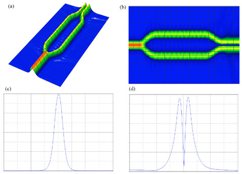 | |
| Fig. 7(a-d): | Result obtained when the input to the quantum NOT gate was state|0,. In this case the NOT gate was built using the electro-optic approach. (a) 3-D view of the optical field (b) 2-D view of the optical field (c) TE0 mode applied at the input (d) TE1 mode at the output |
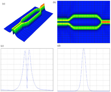 | |
| Fig. 8(a-d): | Result obtained when the input to the quantum NOT gate was state |1〉. In this case the NOT gate was built using the electro-optic approach. (a) 3-D view of the optical field (b) 2D view of the optical field (c) TE1 mode applied at the input and (d) TE0 mode at the output |
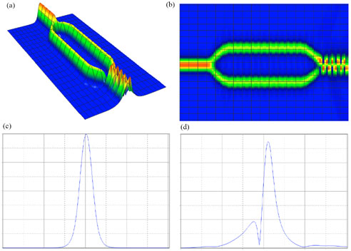 | |
| Fig. 9(a-d): | Results obtained when the input to the |
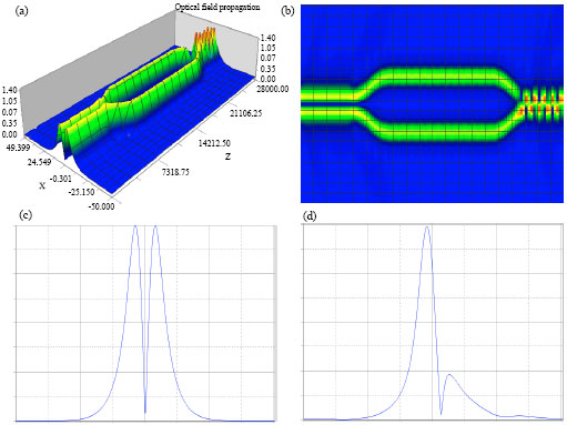 | |
| Fig. 10(a-d): | Results obtained when the input to the |
 | |
| Fig. 11: | Two |
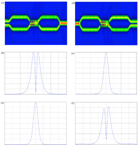 | |
| Fig. 12(a-f): | Verification of |
It would be beneficial if all the Pauli gates could be implemented using this encoding technique because that would facilitate the realization of other gates from it. Emphasis should be given on the implementation of TOFFOLI, CNOT, SWAP and other Controlled gates.
REFERENCES
- Pramono, Y.H. and Endarko, 2001. Nonlinear waveguides for optical logic and computation. J. Nonlinear Opt. Phys. Mater., 10: 209-222.
CrossRefDirect Link - Wu, Y.D., T.T. Shih and M.H. Chen, 2008. New all-optical logic gates based on the local nonlinear Mach-Zehnder interferometer. Opt. Express, 16: 248-257.
CrossRefDirect Link - Wu, Y.D., 2004. Analyzing multilayer optical waveguides with a localized arbitrary nonlinear guiding film. IEEE J. Quantum. Electron., 40: 529-540.
CrossRefDirect Link - Turchette, Q.A., C.J. Hood, W. Lange, H. Mabuchi and H.J. Kimble, 1995. Measurement of conditional phase shifts for quantum logic. Phys. Rev. Lett., 75: 4710-4713.
Direct Link - Cerf, N.J., C. Adami and P.G. Kwiat, 1998. Optical simulation of quantum logic. Phys. Rev. A, 57: R1477-R1480.
Direct Link - Howell, J.C. and J.A. Yeazell, 2000. Reducing the complexity of linear optics quantum circuits. Phys. Rev. Vol. 61.
CrossRefDirect Link - Salemian, S. and S. Mohammadnejad, 2008. Quantum hadamard gate implementation using planar lightwave circuit and photonic crystal structures. Am. J. Applied Sci., 5: 1144-1148.
Direct Link - Okamoto, K., 1999. Recent progress of integrated optics planar lightwave circuits. Opt. Quantum Electron., 31: 107-129.
CrossRef - Salemian, S. and S. Mohammadnejad, 2008. Quantum entanglement implementation using interferometric electro-optic modulator and coupled mode theory. J. Applied Sci., 8: 743-752.
CrossRefDirect Link