
Faten E. Al-Hazmi
Department of Physics, Faculty of Sciences, King Abdul Aziz University, Jeddah 21589, Kingdom of Saudi Arabia
Journal of Applied Sciences
Year: 2011 | Volume: 11 | Issue: 8 | Page No.: 1401-1405


ABSTRACT
The growth and characteristics of wide gap II-VI semiconductor nanowires prepared by the so-called Vapour-Liquid-Solid (VLS) technique was presented ZnSe nanowires were prepared on Si (111) by using Au as catalyst. Vapor-Liquid-Solid (VLS) process under certain conditions to form the desired nanowires. The as-synthesized products were characterized by SEM and EDX. The SEM analysis of ZnSe nanowires indicated that nanowires grow randomly at angles widely different from the vertical.
PDF Abstract XML References Citation
Received: October 19, 2010;
Accepted: December 24, 2010;
Published: March 09, 2011
How to cite this article
Faten E. Al-Hazmi, 2011. Growth and Characterisation of ZnSe Semiconductor Nanowires. Journal of Applied Sciences, 11: 1401-1405.
DOI: 10.3923/jas.2011.1401.1405
URL: https://scialert.net/abstract/?doi=jas.2011.1401.1405
DOI: 10.3923/jas.2011.1401.1405
URL: https://scialert.net/abstract/?doi=jas.2011.1401.1405
INTRODUCTION
Nanotechnology is a cutting age technology and has many potential applications which can be divided into short-term and long-term applications. The short term is to enrich scientific research to develop the characteristics and effectiveness of nano-materials. On the other hand, long term applications is to build nano-devices using atoms and molecules. Nanotechnology is a new branch of engineering, based on the physics of low dimensional structures. This technology increases the ability to design and build devices on an atomic or molecular scale and provides opportunities to develop materials with unique properties. Nanostructured materials are systems in which the physical size in at least one dimension is less than or equal to 100 nm. They are important for both fundamental research applied oriented research since they have the potential to reach far higher device densities compared to traditional material technology. The properties of nanostructures are not only dependent upon dimensionality, but also their physical size.
In semiconducting materials electrons live in a range of define energy level called bands. The conduction band is partially filled band are areas where electrons are missing, known as hole. The advantage of nanotechnology enables much larger surface area hence much more active electrons. The Fermi level (a band gap) are reduced giving advantage to one kind of nanostructured materials is one-dimensional (1D) nanowires. They were first discussed in 1980 (Sakaki, 1980), for application to high electron mobility channels. An important advantage of 1D nanowires over other low dimensional material is that the nanowires can function as both active device elements and interconnects carrying current to and from devices.
Vapor-Liquid-Solid(VLS) process was established in the 1960’s by Wanger and Ellis (1964), later justified thermodynamically and kinetically (Givargizov, 1975). It was recently reexamined and generate nanowires and nanorods from a rich variety of inorganic materials (Shi et al., 2001; Wang et al., 2002; Wu et al., 2002). A typical VLS process starts with the dissolution of gaseous reactants into nanosized liquid droplets of a catalyst metal, followed by nucleation and growth of single-crystalline rods and then wires. The one-dimensional growth is induced and dictated by the liquid droplets, whose sizes remain essentially unchanged during the entire process of wire growth. Each liquid droplet serves as a virtual template to strictly limit the lateral growth of an individual wire.
In this process, the anisotropic crystal growth is promoted by the presence of the liquid alloy/solid interface. The VLS process has now become a widely applied to explain the growth of various nanowires from a rich variety of pure and doped inorganic materials that include elemental semiconductors (He et al., 2001; Duan and Lieber, 2000; Chen et al., 2001) and II-VI semiconductors (Lopez-Lopez et al., 1998; Zhang et al., 2001).
This study premise deals method with fabrication of ZnSe nanowires using VLS process. Stringent control over the conditions of the ZnSe nanowires were identified. This study should help to identify the conditions suitable for fabricating optimized ZnSe nanowires and their associated device (transistor) characteristics. In particular, ZnSe is being actively studied as a result of recent success in the fabrication of blue-green Light Emitting Diodes (LED).
MATERIALS AND METHODS
The experimental setup used in this work is illustrated in Fig. 1.
The furnace is three zone resistance heated furnace (LINDBERG, model 55347-4). Each of the three zones is controlled by a programmable controller with its own thermocouple. Temperature displaying on the controller panels and of sample inside furnace may be different because thermal couple connected with controller is located in outside tube. The maximum working temperature can be set to 1100°C.
Temperature calibration: In order to achieve accurate temperature inside tube during heating, we should calibrate tube furnace. First determine the temperature profile in the growth tube using condition similar to growth.
Cleaning of the substrate: Clean Si substrates using acetone follow by ethanol and deionised water. Ultrasonic is preferred. When Si substrates had their native oxide removed by etching them in 10% HF/H2O followed by a very short Di water rise.
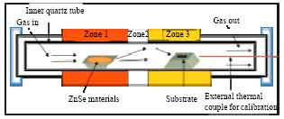 | |
| Fig. 1: | A schematic diagram of the experimental setup for synthesis of II-VI semiconductor nanowires |
Deposition of catalyst film: The Si substrates coated with a 30 nm thick layer of Au film by thermal evaporation.
Loading the furnace: The source material in this work is ZnSe powder (Alpha Aesar) placed in an alumina boat. The source is placed at 965°C and the substrate with Au film is placed at 750°C. Prior to heating, the system was first evacuated to about 100Torr and then flushed with a high flow of Ar gas (flow rate = 100 sccm) for almost 1 h to eliminate oxygen traces from the growth chamber.
RESULTS AND DISCUSSION
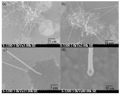
Figure 2a-d show the typical low and high magnification SEM images of ZnSe nanowires grown on Si (111) with thin Au film. The image shows that the nanowires are formed on the substrate in high yield.
Nanowires were identified by energy dispersive X-ray spectroscopy (EDXS), where the EDXS analysis provided precise composition of the tip. Figure 3 show the EDXS spectra, feature peaks corresponding to elements Au, Si, Zn and Se peaks, which depict the characteristic composition of a tip of a nanowires.
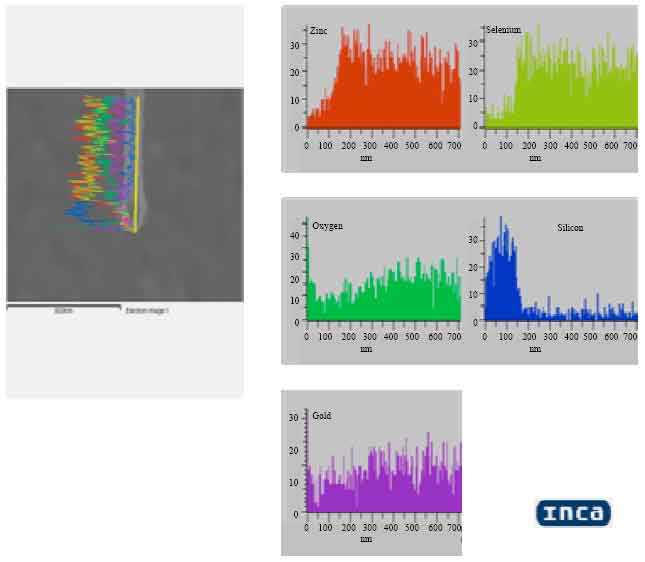
An elemental mapping of the nanowires composition along the length of these nanowires further confirming its stoichiometric composition is shown Fig. 4.
Finally, we growth ZnSe nanowires vertically against the gravity. Figure 5, shows the typical (a and b) low and (c and d) high-resolution SEM images ZnSe nanowires grown against the gravity on Si (111) with thin Au film.
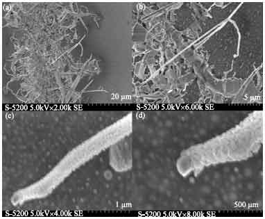 | |
| Fig. 2: | The typical (a and b) low and (c and d) high-resolution SEM images ZnSe nanowires |
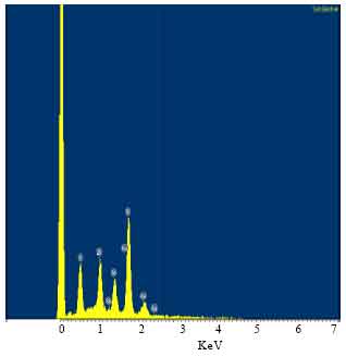 | |
| Fig. 3: | EDXS spectrum confirming the chemical composition of ZnSe nanowires |
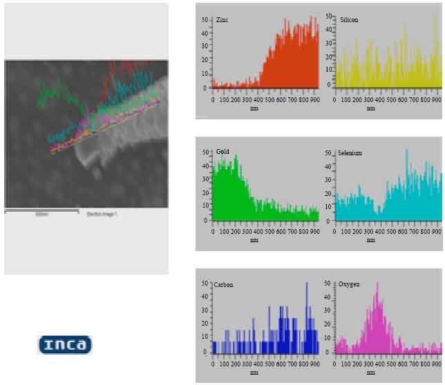 | |
| Fig. 4: | Element mapping of ZnSe nanowires confirming its composition along its length |
 | |
| Fig. 5: | The typical (a and b) low and (c and d) high-resolution SEM images ZnSe |
 | |
| Fig. 6: | Vertical element mapping of ZnSe nanowires confirming its composition along its length |
The vertical elemental mapping of the nanowires composition along the length of these nanowires is shown in Fig. 6. The results of ZnSe growth is very much anisotropic rather than gravity.
CONCLUSION
In summary, we have synthesized ZnSe nanowires on Si(111) substrate by VLS growth process using Au as catalyst. The SEM analysis of ZnSe nanowires indicated that nanowires grow randomly at angles widely different from the vertical.
ACKNOWLEDGMENTS
I would like to express my gratitude to Professor Harry Ruda for his support and continual guidance and friendly supervision during my period of summer training, Center for Nanotechnology, University of Toronto, Canada). Finally I am grateful to King Abdul-Aziz City for Science and Technology (KACST) for offering my summer training.
REFERENCES
- Chen, C.C., C.C. Yeh, C.H. Chen, M.Y. Yu and H.L. Liu et al., 2001. Catalytic growth and characterization of gallium nitride nanowires. J. Am. Chem. Soc., 123: 2791-2798.
PubMed - Duan, X. and C.M. Lieber, 2000. General synthesis of compound semiconductor nanowires. Adv. Mater., 12: 298-301.
CrossRef - He, M., P. Zhou, S.N. Mohammad, G.L. Harris and J.B. Halpern et al., 2001. Growth of GaN nanowires by direct reaction of Ga with NH3. J. Crystal Growth, 231: 357-365.
CrossRef - Lopez-Lopez, M., A. Guillen-Cervantes, Z. Rivera-Alvarez and I. Hernandez-Calderon, 1998. Hillocks formation during the molecular beam epitaxial growth of ZnSe on GaAs substrates. J. Cryst. Growth, 193: 528-534.
CrossRef - Sakaki, H., 1980. Scattering suppression and high-mobility effect of size-quantized electrons in ultrafine semiconductor wire structures. Jpn. J. Applied Phys., 19: 735-738.
CrossRef - Shi, W.S., Y.F. Zheng, N. Wang, C.S. Lee and S.T. Lee, 2001. Synthesis and microstructure of gallium phosphide nanowires. J. Vac. Sci. Technol. B, 19: 1115-1118.
CrossRefDirect Link - Wanger, R.S. and W.C. Ellis, 1964. Vapor-liquid-solid mechanism of single crystal growth. Applied Phys. Lett., 4: 89-89.
CrossRef - Wang, Y., L. Zhang, C. Liang, G. Wang and X. Peng, 2002. Catalytic growth and photoluminescence properties of semiconductor single-crystal ZnS nanowires. Chem. Phys. Lett., 357: 314-318.
CrossRef - Wu, Y., H. Yan, M. Huang, B. Messer, J.H. Song and P. Yang, 2002. Inorganic semiconductor nanowires: Rational growth, assembly and novel properties. Chem. A Eur. J., 8: 1260-1268.
CrossRefDirect Link - Zhang, J., X.S. Peng, X.F. Wang, Y.W. Wang and L.D. Zhang, 2001. Micro-Raman investigation of GaN nanowires prepared by direct reaction Ga with NH3. Chem. Phys. Lett., 345: 372-376.
CrossRef