
M. Azaga
M. Othman
Journal of Applied Sciences
Year: 2009 | Volume: 9 | Issue: 4 | Page No.: 738-744


ABSTRACT
A proposed design of Ultra Wideband (UWB) pulse generator circuit is presented. The design is based on Source Couple Logic (SCL) for its low power and high immune to noise so it can be used in mixed signal ICs environment. The pulse is digitally generated by using SCL inverters and NAND gates; the output of clock pulse input is dual pulse signals opposite to each other. The design is simulated and result of the circuit is dual pulses with width of sub-nanosecond. The results gotten have satisfied the design idea as desired. Post simulation has been carried out by using HSPICE, the layout is done using Cadence Virtuoso and verification is done by Mentor Graphic Interactive tool. All simulations are based on MIMOS 0.35 μm process PDK.
PDF Abstract XML References Citation
How to cite this article
M. Azaga and M. Othman, 2009. Physical Design of Source Couple Logic Pulse Generator Circuit for Ultra Wideband Applications. Journal of Applied Sciences, 9: 738-744.
DOI: 10.3923/jas.2009.738.744
URL: https://scialert.net/abstract/?doi=jas.2009.738.744
DOI: 10.3923/jas.2009.738.744
URL: https://scialert.net/abstract/?doi=jas.2009.738.744
INTRODUCTION
Ultra Wideband (UWB) radio is defined as a wireless technology to transmit data over very wide spectrum of frequency bands with very low power (Kim and Park, 2003). It’s capable of carrying extremely high data rates over a short distance (e.g., <15 m) with very good communication features (Silverstrim, 2003; Intel, 2004; Heydari, 2007; Luo and Yang, 2003). For that UWB radio (impulse radio) becomes more interesting from industry, government and academic institutes.
The first considerations in the designing UWB circuits and system is choosing a proper impulse signal type for the UWB radio, since the impulse type determines the performance level of the UWB systems (Taylor, 1994). The selected waveform for UWB system has to provide the best transferring capacity and must have low interference characteristics to enable a high data transferring rate and wide operation range. Also, implementing the pulse circuit on a chip could be other benefits for commercial product (Jeong and Jung, 2004). Different types of pulse-generation/shaping algorithm for UWB system are proposed by Lee and Nguyen (2001), Luo and Yang (2003), Marsden and Lee (2003), Parr et al. (2003), Dilmaghan et al. (2004) and Jeong and Jung (2004), also, circuit implementation (Lee and Nguyen, 2001; Marsden and Lee, 2003; Dilmaghan et al., 2004; Jeong and Jung, 2004) and coherent and noncoherent receiver architectures using these pulses have been presented by Dmitriev et al. (2003) and Oh et al. (2005).
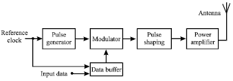 | |
| Fig. 1: | Typical UWB transmitter |
The use of digital filters in the shaping are flexible in terms of programmability, but the complexity and requirements for very high-speed clock building blocks make their implementation nontrivial. Because of the difficulties encountered in implementing digital filters, most of the pulse generation circuits are based on analog pulse generator circuit.
The typical pulsed UWB transmitter shown in Fig. 1 is composed of different basic blocks as the following: pulse generator to produce a Gaussian monocycle pulse, modulator for encoding, impulse shaping to shape the pulse to fit the FCC UWB required mask and power amplifier to amplify the modulated signal for transmitting antenna. All designed pulse generation circuit which refereed before use standard CMOS as basic building elements.
The basic concerns of this study is to design a pulse generation block with emphasis on low-power concepts and immune to digital noise in mixed signal environment. The proposed design introduces a new efficient-power, high stability pulse generator circuit using Source Couple Logic (SCL) technique by mean of delay line and, a NAND gate. The SCL is promising high speed efficient-power consumption logic comparing to the conventional CMOS logic. It had shown to be an interesting alternative logic style than the traditional static CMOS logic in many applications (Allstot and Chee, 1993; Kundan and Hasan, 2000; Alioto and Palumbo, 2003; Khabiri and Shams, 2004; Kwan and Shams, 2004). Indeed, even if the basic drawback of SCL gates is to have static power consumption, they are faster and show a better power efficiency than standard CMOS gates in high-speed applications (Maskai and Kiaei, 1992; Allstot and Chee, 1993; Kundan and Hasan, 2000; Alioto and Palumbo, 2003). In addition, SCL gates generate a much lower switching noise, thus they dramatically reduce the digital noise induced on the analog circuits in mixed-signal applications and inherently have a better signal integrity (Khabiri and Shams, 2004; Kwan and Shams, 2004). As another potential advantage which is currently under investigation, SCL circuits have a lower sensitivity to process variations (Allstot and Chee, 1993; Srinivasan and Ha, 2004). Hence, SCL circuits are less sensitive to the limitations arising from the technology scaling; therefore, they are an interesting logic style in digital/mixed-signal ICs in sub-100 nm technologies. The output of impulse generation block is a narrow pulse that comply the UWB pulse specification (usually in rang of sub-nanoseconds (Han et al., 2003). This study concern mainly the pulse generation circuit block.
PULSE GENERATION CIRCUIT
The Pulse Generation Circuit (PGC) is based on idea of comparing two pulses, one delayed to another and generating a pulse by amount of time difference in between as shown in Fig. 2. This is done digitally by means of comparing two signals, original signal and its delayed version, using NAND gate which output the difference pulse.
To implement this idea, PGC is proposed as shown in the Fig. 3, the inverter and NAND gates are designed using SCL. The PGC is composes of different blocks and parts as shown in Fig. 3. Beginning, since SCL is dual mode logic, a designed circuit is needed to change from single-mode to dual-mode logic which done by single-to-dual converter block which outputs dual opposite pulses which required by SCL. The output of pulse generator circuit is ready dual-pulse (+ve and -ve) which can be utilized for encode the transmitted data using pulse polarity coding scheme (+1 and -1) and this is considered one of the advantages of using SCL.
The input to the PGC is single clock pulse, (A in the Fig. 2) repetition frequency is converted to dual pulses as needed by SCL (B and C), the single-to-dual converter is designed by mean of CMOS inverter and Transmission Gate (TG). Figure 4 connected in parallel to get same delay on the dual opposite output signals, then, its connected to the SCL Inverter in order to get desired ΔV to other SCL gates in the PGC.
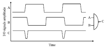 | |
| Fig. 2: | Pulse generation data |
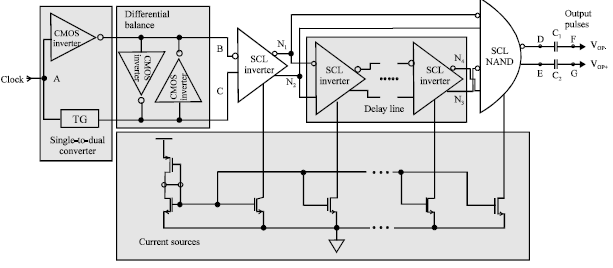 | |
| Fig. 3: | Pulse generation circuit topology |
To have balance switching and same slew rate, the outputs of single-to-dual converter block are connected differentially by means of two CMOS inverter, one opposed the other, as shown in the differential balance block in Fig. 3.
The output dual-signals of SCL inverter are inputted to the delay line and SCL NAND gate at the same time. The delay line is consisting of odd/even number of SCL inverters; therefore, the output of the delay line (N3 and N4) is delayed inverted original input signals N1 and N2. The amount of delay is multiple delay of the used SCL inverter, the delay of delayed signal will give the width of output pulses from pulse generation block (D and E), since it’s input to 2-inputs SCL-NAND with original dual signals (N1 and N2), the output of SCL-NAND will goes high as one of the input signals is low. To get inverted signal at second dual inputs of SCL-NAND for comparison, attention must be taken for connecting of N3 and N4 to the SCL-NAND, that is depending on the number of SCL inverter in the delay line, odd/even, if it’s odd, the connection will be directly-true to true and false to false, where, if it’s even, the connection will be inversed - true to false and false to true-as in Fig. 3.
The TG and CMOS inverter are shown in Fig. 4a, b sized in such a way that the output signal has same rising and falling time during switching.
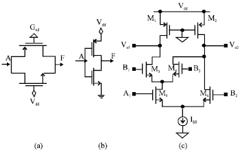 | |
| Fig. 4: | (a) TG, (b) CMOS inverter and (c) SCL-NAND |
The schematic diagram of SCL-NAND gate used in the PG circuit is shown in Fig. 4c. The coupling capacitor C1 and C2 are used to remove the DC component of the output signals (F and G).
The PMOS in the inverters and NAND should be sized to get the desired output voltage swing (ΔV), where as NMOS sized to have good noise margin (Azaga and Othman, 2006). As SCL gate needs a current to be steered to one of output branches, a current mirror is used as current source connected to the SCL gates to draw the gate current. Normal current mirror is used with diode connected NMOS as current source reference for the current mirror (Allen and Holberg, 2002). The value of current is affecting the ΔV and delay of SCL gate, so, it’s sited to get low gate delay and desired ΔV (Azaga and Othman, 2006).
PHYSICAL DESIGN OF PGC
The way of layout the SCL gates have effective affect on its performance from point of voltage swing and switching noise, signal delay, as well as utilized area, that is due of introduced RC parasitic (Azaga and Othman, 2006). Four ways of layout are suggested by Azaga and Othman (2006) for SCL gates, among them, fingering and comb layout techniques have been chosen for PGC layout as they have different parasitic effect and to investigate the influence of layout technique over the PGC output signals characteristics. The layout of PGC was done by two versions, using fingering technique (layout I) as in Fig. 5 and using comb technique (layout II) as shown in Fig. 6, which clearly illustrate the reduction of PGC size by the second layout to approximately half of the first layout. The layout is done based on 0.35 μm MIMOS PDK and using Virtuoso-Cadence, where, the extraction is done by Mentor Graphic-Caliber interactive tool.
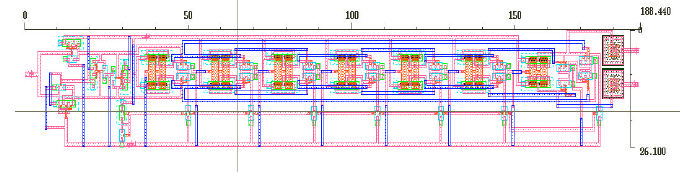 | |
| Fig. 5: | Layout I: Fingering technique |
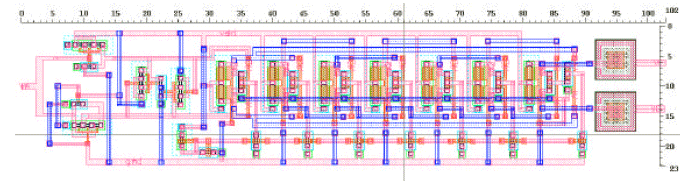 | |
| Fig. 6: | Layout II: Comb technique |
 | |
| Fig. 7: | (a and b) Output pulses from single-to-dual converter block for all PGC models |
SIMULATION RESULTS
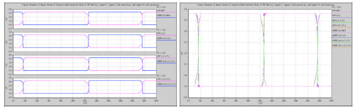
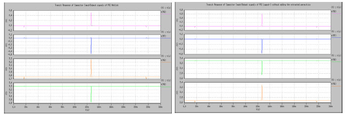
The PGC was designed digitally using SCL gates which considered high noise immune in the mixed signal ICs environment. Physical (Post) simulation is carried out using HSPICE on PGC netlist as well as extracted layouts. Four models of PGC has been considered in post simulation phase, PGC netlist, PGC layout-I pure, PGC layout I with added extracted parasitic and PGC layout II with added extracted parasitic, arranged, respectively where mentioned. The input reference clock pulse to the PGC (VA) is fixed in all post simulation with frequency of 5 MHZ, 10 nsec rise/fall time, 10 nsec delay and 0 to 3.3 V voltage range. VA is then converted to dual signals (VB and VC) by CMOS inverter and TG of the single-to-dual converter block, Fig. 7a and b shows the outputs of single-to-dual converter block of all PGC models.
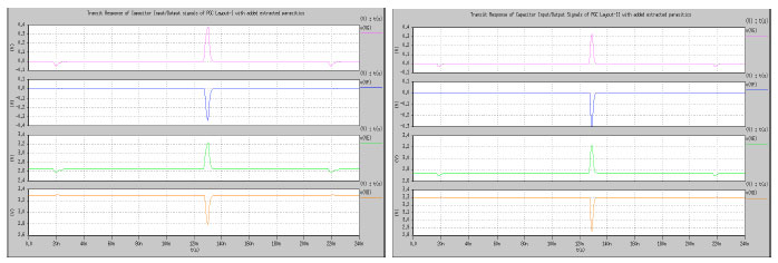
The dual pulse signals VB and VC are input to a SCL inverter in order to achieve desired ΔV for subsequent PGC stages. The SCL inverter’s output is applied parallelly to SCL-NAND and delay line, the delay line composes of odd number of SCL inverters. At the input ports of SCL-NAND (N1, N2, N3 and N4) are the original signals and its delayed inverted copy (Dual) as shown in Fig. 8a and b.
 | |
| Fig. 8: | (a and b) Inputs pulses to SCL NAND (N1, N2, N3 and N4) for all PGC models, Netlist, Layout-I pure, Layout-I, and Layout II, respectively |
 | |
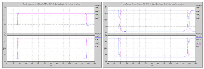
| Fig. 9: | (a-d) Output pulses from SCL NAND (VG,VF,VE and VD) for all PGC models, respectively |
The outputs of SCL NAND are dual inverted short impulse signals with added some DC voltage because of SCL ΔV is part of full headroom voltage. The width of output impulses is based on the amount of delay causes by the delay line to the original dual signals. The DC voltage is removed by using capacitors at the output of SCL-NAND. Figure 9a-d, shows the input/output impulse signals of capacitors for four simulations models of PGC.
The four models of PGC output four different dual short impulses, as shown in Fig. 10. The shown characteristics of PGC output signals are fitting UWB pulse duration constrain as required, but the difference in pulse characteristics are due to parasitic effect on circuit behavior. The amount of RC parasitics added to the circuit layout has major impact on signal strength and delay.
The output pulses of PGC Netlist and layout I pure are showing less delay to middle falling edge of VA than layout I and II with parasitic, a mostly it’s close to middle falling edge of VA. The PGC Netlist is considering only the devices models as in the PDK. The peak voltage of PGC layout I pure output signals is more than PGC layout I and II with added parasitic because no parasitic capacitance/resistance is added, only the physical layout of the devices is considered with its resistance/ capacitance, which less than the total layout capacitance/ resistance parasitic, that is raise slightly the ΔV than PGC Netlist and others.
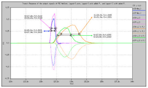 | |
| Fig. 10: | The output pulses of PGC (all models) |
| Table 1: | The main output pulses parameters of different PGC models |
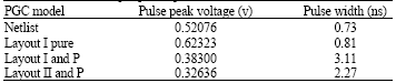 | |
PGC Layout-I with added parasitic shows more width and peak voltage of output pulses than PGC layout II with added parasitic due to increasing of it is nodes and paths capacitance as well as decreasing resistance values. Both, PGC Layout-I and Layout-II with added parasitic output signals have same delay to the VA due of signals paths capacitance. Table 1 shows the main parameters of the four PGC models output pulse signals.
CONCLUSION
The PGC was digitally designed by using SCL gates, that suitable to use in mixed signal ICs environment. SCL inverters are used in delay line to delay the input signal, where, 2-inputs SCL-NAND were used to get difference between the original and delayed signals. In the design, 5 stages of SCL-Inverters used as delay line, the amount of delay is controlled by the total delay of the delay line and by increases the delay elements the total delay can be increased, so the output pulse width from SCL-NAND. Extensive simulation is done to adjust W/L for all CMOS in PGC blocks to get best output pulse and apply the SCL design constrains at same time. Four models of PGC are considered for investigation, two different layout techniques were considered in post simulation. The simulation results show important effect of layout on output pulses characteristics and all PGC performance. All output pulse signals of all PGC models are short impulse width in sub-nanosecond which fit the UWB pulse width constrain (Han et al., 2003). All post simulation is carried out by HSPICE and using MIMOS 0.35 μm process PDK. The fabrication of layout-I and layout-II PGCs is under processing and the measurements shall be discussed and explored in the further study,
ACKNOWLEDGMENTS
We would like to thank MIMOS Berhad for all its support and offering all study facilities. Also, we do not forget to thank mixed analog signal group in Microelectronics and MEMS Department at MIMOS for all their help and support.
REFERENCES
- Alioto, M. and G. Palumbo, 2003. Design strategies for source coupled logic gates. IEEE Trans. Circuits Syst. I: Fundamental Theory Appl., 50: 640-654.
CrossRefDirect Link - Allen, P.E. and D.R. Holberg, 2002. CMOS Analog Circuit Design. 1st Edn., Oxford University Press, USA.
Direct Link - Allstot, D.J. and S.H. Chee, 1993. Folded source-coupled logic vs. cmos static logic for low-noise mixed-signal ics. IEEE Trans. Circuits Syst. I: Fundamental Theory Appl., 40: 553-563.
Direct Link - Dilmaghan, R.S., M. Ghavami and A.H. Aghvami, 2004. UWB multiple-pulse generator and transmitter. Procceding of the International Workshop on Ultra Wideband Systems, 2004. Joint with Conference on Ultrawideband Systems and Technologies, Joint UWBST and IWUWBS, May 18-21, 2004, Beijing, pp: 117-121.
CrossRefDirect Link - Dmitriev, A.S., A.I. Panas and K.V. Zakharchenko, 2003. Basic principles of direct chaotic communications. Interdisciplinary J., 6: 488-501.
Direct Link - Han, J.W., M. Miao and N. Cam, 2003. Recent development of srd and fet based sub-nanosecond pulse generators for ultra-wideband communications. Proceedings of the Topical Conference on Wireless Communication Technology, October 15-17, Honolulu, pp: 441-442.
CrossRef - Heydari, P., 2007. Design and analysis of a performance-optimized CMOS UWB distributed LNA. IEEE J. Solid State Circuits, 42: 1892-1905.
Direct Link - Jeong, Y. and S. Jung, 2004. A CMOS impulse generator for uwb wireless communication systems. Proceedings of the International Symposium on Circuits and Systems, May 23-26, 2004, Piscataway, New Jersey, pp: 129-132.
Direct Link - Kim, H. and D. Park, 2003. Design of CMOS scholtz's monocycle pulse generator. Proceedings of the Conference on Ultra Wideband Systems and Technologies, November 16-19, 2003, Tempe, AZ., USA., pp: 81-85.
CrossRef - Kundan, J. and S.M.R. Hasan, 2000. Enhanced folded source-coupled logic technique for low-voltage mixed-signal integrated circuits. IEEE Trans. Circuits Syst. II: Analog Digital Signal Proc., 47: 810-817.
CrossRef - Kwan, T.W. and M. Shams, 2004. Multi-GHz energy-efficient asynchronous pipelined circuits in MOS current mode logic. Proceedings of the International Symposium on Circuits and Systems, May 23-26, 2004, IEEE Piscataway, New Jersey, pp: 645-648.
Direct Link - Lee, J.S. and C. Nguyen, 2001. Novel low-cost UWB, ultra-short-pulse transmitter with MESFET impulse-shaping circuitry for reduced distortion and improved pulse repetition rate. IEEE Microwave Wireless Components Lett., 11: 208-210.
Direct Link - Luo, X. and L. Yang, 2003. Designing optimal pulse-shapers for ultra-wideband radios. J. Commun. Networks, 5: 349-353.
Direct Link - Marsden, K. and H.J. Lee, 2003. Low power CMOS re-programmable pulse generator for UWB systems. Proceedings of the Conference on Ultra Wideband Systems and Technologies, November 16-19, 2003, Reston, Virginia, pp: 443-447.
CrossRefDirect Link - Maskai, S.R. and S. Kiaei, 1992. Synthesis techniques for CMOS folded source-coupled logic circuits. IEEE J. Solid State Circuits, 27: 1157-1167.
Direct Link - Oh, M.K., B. Jung, R. Harjani and P. Dong-Jo, 2005. A new noncoherent UWB impulse radio receiver. IEEE Commun. Lett., 9: 151-153.
Direct Link - Parr, B., B. L. Cho, K. Wallace and D. Zhi, 2003. A novel UWB pulse design algorithm. IEEE Commun. Lett., 7: 219-221.
Direct Link - Srinivasan, V. and D.S. Ha, 2004. Gigahertz-range MCML multiplier archituctures. Proceedings of the International Symposium on Circuit and Systems, May 23-26, 2004, IEEE, Piscataway, New Jersey, pp: 785-788.
Direct Link