
Pouya Asadi
Islamic Azad University Science and Research Branch, Tehran, Iran
Keivan Navi
Faculty of Electrical and Computer Engineering, Shahid Beheshti University, Tehran, Iran
Journal of Applied Sciences
Year: 2007 | Volume: 7 | Issue: 18 | Page No.: 2629-2634


ABSTRACT
We propose a 32x32-bit multiplier with reduced delay compared to conventional multiplication algorithms. An efficient radix-2 recording logic generates the partial products. A 2-phase micro pipeline latch controller is used which controls a 4-phase pipeline with standard transparent level sensitive latches. The design employs the modified Booth algorithm diminishing 8 bits at a time with an iterative structure. Assign extension algorithm is also employed in this study. Furthermore, the early termination scheme speeds up the multiplication operation. The multiplication time is 3.1 n sec at a 1.3-V power supply. Present multiplication algorithm showed 13% speed improvement, 14% power savings and 9.5% reduction in transistor count when compared to the conventional multiplication algorithms.
PDF Abstract XML References Citation
How to cite this article
Pouya Asadi and Keivan Navi, 2007. A New High-Speed Low Power Consumption Multiplier. Journal of Applied Sciences, 7: 2629-2634.
DOI: 10.3923/jas.2007.2629.2634
URL: https://scialert.net/abstract/?doi=jas.2007.2629.2634
DOI: 10.3923/jas.2007.2629.2634
URL: https://scialert.net/abstract/?doi=jas.2007.2629.2634
INTRODUCTION
The performance of 3D graphics and signal processing systems strongly depends on the performance of multiplications because these applications need to support operations that are highly multiplication-intensive. Therefore, there has been much study on advanced multiplication algorithms and designs (Kang and Gaudiot, 2004). In typical processes, multiplication takes between two and eight cycles (Itoh et al., 2006). Consequently, having high-speed multipliers is critical for the performance of processors. Processor designers have recognized this and have devoted considerable silicon area for the design of multipliers (Goodman and McAuley, 2006). Recent advances in integrated circuit fabrication technology have resulted in both smaller feature sizes and increased die areas.
Asynchronous logic gained a resurgence of interest among academic and industrial researchers due to its advantages in low power consumption, high operating speed, less emission of electromagnetic noise (EMI), better compensability and avoiding clock skew problems (Kang and Gaudiot, 2004). Synchronous design uses global clock to control dataflow in the data path. A clocked system can be viewed as a Finite-State Machine (FSM) with registers (flip-flops) holding the current state. The clocked system changes from one state to the next state on the edges of the global clock. The state is held in a set of registers and combinatorial logic is used to derive a new state and outputs. The new state is copied through the registers on every rising or falling edge of the global clock signal. Asynchronous logic uses a different timing stratagem handshaking protocol. There are two common handshaking protocols used by self-timed systems: 4-phase protocol (Itoh et al., 2006) and 2-phase protocol (Goodman and McAuley, 2006). Unlike 4-phase protocol, which uses level-sensitive control signals, 2-phase protocol employs events (rising or falling edges) to indicate the availability or absorption of data. The 4-phase protocol has better adaptability to most of VLSI designs but its superfluous return-to-zero transitions cost unnecessary time and energy. In this study, we propose an asynchronous pipelined multiplier using a 2-phase pipeline control circuit to control a 4-phase data path with level sensitive latches. Thus, we can keep the advantage of 4-phase protocol but gain a faster and lower power result.
MATERIALS AND METHODS
This study started in 2005 at Microelectronic Center of Islamic Azad University Science and Research Branch and Faculty of Electronic and Computer Engineering, Shahid Beheshti university. Compared to 2-phase protocol, 4-phase protocol has better adaptability because most VLSI designs use level sensitive data path. The asynchronous circuits using 4-phase handshaking protocol can easily use transparent latches in the pipeline without two-to four-phase signaling converters.
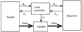 | |
| Fig. 1: | Block diagram hybrid latch controller |
While 2-phase handshaking protocol is faster and costs lower power because it eliminates the superfluous return-to-zero transitions. The motivation of employing the hybrid handshaking protocol is to combine the advantages of both 4-phase protocol and 2-phase protocol. Figure 1 illustrates the block diagram of a hybrid latch controller. Rin is the request signal from the sender and Rout is the request signal to the receiver. While Ain is the acknowledge signal to the sender and Aout is the acknowledge signal from the receiver. Lt is the control line, which controls the states of level sensitive latches. The control flow of the latch controller using hybrid handshaking protocol is shown as follows:
At the beginning, Lt controls the state of latches as transparent (open). After the sender sets up data, it issues an event on Rin indicating the validity of data. The latch controller changes the state of latches to opaque (close) and let them absorb the data. Then the latch controller sends an event on Ain back to the sender to acknowledge the capture of data. At the same time, it issues an event on Rout to indicate the availability of data. After some time, the latch controller detects an event on Aout form the receiver and it changes latches to transparent state again to prepare next cycle of data transmission. By choosing different events (rising or falling edge), control circuits can be composed by different ways. The Signal Transition Graph (STG) (Ohkubo et al., 1995) description of a latch controller is shown in Fig. 2. By a synthesis tool-Petrify (Twagiry and Flynn, 2004), we can easily synthesize the latch controller from the STG description. The latch control circuit generated by Petrify is shown in Fig. 3. However, this circuit looks too big and not optimal. A better latch controller called mousetrap is proposed by (Cheng and Theobold, 2000). In this study, we use mousetrap as the latch controller to control the micro pipeline.
Multiplier architecture: Array multipliers (Hoon and Jun, 2002) and tree multipliers (Huang and Ercegovac, 2005) are rather fast but, on the other hand, are rather hardware hungry. Serial multipliers (Liu, 2003) need less area but have a very low throughput. Iterative multipliers are good choice considering the tradeoff between speed and silicon area.
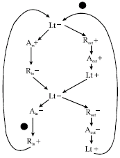 | |
| Fig. 2: | STG description of a latch controller |
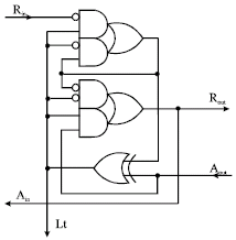 | |
| Fig. 3: | Latch controller implementation |
With pipeline technique, iterative multipliers can gain an equal throughput as that of parallel multipliers if we ignore the delay of registers or latches (Kyoung, 2003).
The multiplier of (Wang and Miller, 2005) uses a synchronous pipeline structure clocked by an inverter oscillator. Compared to synchronous pipeline, self-timed pipeline has three main advantages:
Higher speed: Asynchronous pipeline uses handshaking protocol and it operating speed is determined by actual combinational logic block latencies of each stage rather than the critical delay of all the stages.
Less silicon area: Standard transparent latches are used in asynchronous pipeline whereas synchronous pipeline must employ edge-trigged registers to hold stages. Edge trigged registers occupy double silicon space compared to transparent latches. Furthermore, transparent latches are two times faster than edge-trigged registers, which furthers self-timed the pipeline's advantage in high speed.
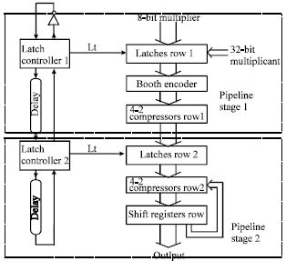 | |
| Fig. 4: | Multiplier micro pipeline structure |
More robust: Only after the availability and capture of data, will the sender and the receiver send the request and acknowledge signals. While a synchronous pipeline should satisfy the critical delay of all the stage circuits, which perhaps changes from time to time. For example, there comes a bug when the (Kang and Gaudiot, 2006) multiplier changes its state from normal calculation to early termination.
The Multiplier in this paper uses modified booth algorithm and supports 32x32-bit integer multiplication of both signed and unsigned operands. The multiplier architecture is illustrated in Fig. 4. This is a two-stage asynchronous pipeline structure using bundled-data protocol. The first stage includes a booth encoder, a pipeline latches row and a 4-2 compressors row. The second stage includes a pipeline latches row, a 4-2 compressors row and a shift registers row. The pipeline latch controllers are mouse-trap introduces next.
Booth’s algorithm: Booth’s encoder is shown in Fig. 5a, The multiplicands, Y2i-1, Y2i, Y2i+1 are encoded by this circuit. Encoding the data halves the number of partial products. The simulated propagation delay time is 0.50 n sec. The partial-product generator is shown in Fig. 5b. A multiplier, either Xj or Xj-1, is selected depending on whether encoded data, X or 2X is high and inverted by encoded data, NEG. The simulated propagation delay time is 0.56 n sec.
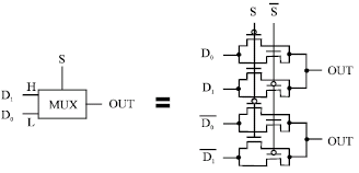
Pass transistor multiplexer: The pass-transistor multiplexer used in the 4-2 compressor is shown in Fig. 6. When the control signal S is low, data D0 is selected and when the control signal S is high, data D1 is selected.
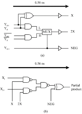 | |
| Fig. 5: | Booth's algorithm: (a) Booth's encoder, (b) Partial product generator |
 | |
| Fig. 6: | Pass transistor multiplexer circuit |
The output is used as the control signal input for the next-stage multiplexer. Thus, the multiplexer has both positive and negative output. It can reduce the propagation delay by eliminating an inverter.
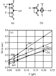
Several pass-transistor logic circuits have been proposed to improve the performance of CMOS circuits. The NMOS pass-transistor logic circuits (Itoh et al., 2006) is one example. It has been shown to result in high speed due to its low input capacitance and high logic functionality. However, particularly in reduced supply voltage designs, it is important to take into account the problems of noise margins and speed degradation. These are caused by mismatches between the input signal levels and the logic threshold voltage of the CMOS gates, which fluctuates with process variations.
 | |
| Fig. 7: | Comparison of CMOS and pass-transistor circuits: (a) CMOS tristate inverter, (b) Pass-transistor tristate inverter, (c) Comparison of delay time |
To avoid these problems, the multiplexer in this design consists of both NMOS and PMOS pass transistors.
The delay time of the pass-transistor multiplexer is shorter than that of a CMOS gate, because of the pass-transistor based design where both the NMOS and PMOS are turned on. The CMOS tristate inverter and pass-transistor tristate inverter are shown in Fig. 7a and b, which are used in CMOS and pass-transistor multiplexers, respectively. The number of transistors in both circuits is the same and both have equal input capacitance. A simulated comparison is shown in Fig. 7c, showing the dependence of the delay time from in to out on the output load capacitance. The low driving source impedanceattained by using the pass transistor makes the delay time of the pass-transistor shorter than that of a CMOS gate.
4-2 Compressor circuit: The 4-2 compressor circuits using pass-transistor multiplexers are shown in Fig. 8. The signal lines in the figure represent positive and negative signals. The inputs of the multiplexers are either two different signal, or one signal and logical invert. All outputs (S, C and C0) have buffers to enhance driving ability. The 4-2 compressor circuits add four partial products (I1-I4) and generate a sum signal (S) and two carry signals (C and C0).
Since the pass-transistor multiplexer circuit shown in Fig. 6 has high logic functionality, a full-adder circuit is constructed from three pass-transistor multiplexers. The 4-2 compressor is constructed from two full adders, such that there are four critical path gate stages, as shown in Fig. 8a.
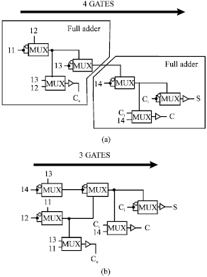 | |
| Fig. 8: | 4-2 compressor circuits using pass-transistor multiplexers: (a) Full-adder-based construction (b) Proposed construction |
This circuit is faster than conventional CMOS circuits due to the use of pass-transistor multiplexers.
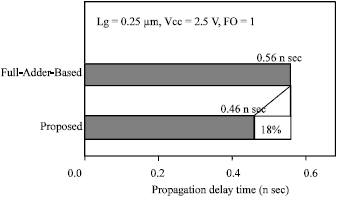
For further speed improvement, we developed a new 4-2 compressor. Though the number of multiplexers is the same, the number of critical-path gate stages in this circuit is reduced to three by exploiting parallelism, as shown in Fig. 8b. In this new configuration, the carry-out (C0) does not depend on the carry-in (Ci), so, the advantage of the 4-2 compressor is maintained with this new configuration. The simulated delay comparison for these 4-2 compressor circuits is shown in Fig. 9. The propose circuit reduces the propagation delay time by 18% from that of a full-adder-based circuit.
Pipeline latch and shift register: Considering both speed and hardware consumption we choose True Single-Phase Clocking (TSPC) register to compose the shift register row. The pipeline latches are normal transparent latches, which is very simple and fast. The schematic of TSPC register is illustrated in Fig. 10.
Simulation: The multiplier was analyzed using HSPICE on extracted layout under conditions of 1.3-volt supply voltage and 100 degree temperature. The simulation results of delay (Typical process case and Worse process corner) are given in Table 1.
 | |
| Fig. 9: | Simulated comparison of 4-2 compressor circuits |
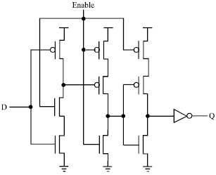 | |
| Fig. 10: | The schematic of TSPC register |
| Table 1: | Simulated results of the components delay |
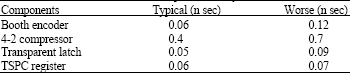 | |
| ns: Nano second | |
The critical path of the first pipeline stage includes one Booth MUX, one 4-2 compressor and one pipeline latch and is totally equal to 1.04 n sec (Under the worst-case conditions: Vdd = 1.3 v, Vss = 0.1 v, 100 degree temperature). The critical path of the second pipeline latch, one 4-2 compressor and one shift TSPC register and is totally equal to 0.42 n sec. it takes 3.1 n sec to complement a 32x32-bit multiplication without using early termination. With 20% commercial timing margin, the multiplier completes a multiplication in 4.1 n sec under worst-case conditions. The power of this study is about 4.4 mW with full load in peak time and the average power is about 2.4 mW.
CONCLUSIONS
A high performance, low hardware cost and low power asynchronous iterative multiplier has been developed in this study.
| Table 2: | Comparison between 32x32 bit multipliers |
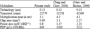 | |
| μm: Micro meter; ns: Nano second; MHZ: Mega hertz | |
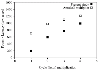 | |
| Fig. 11: | The comparison of powerxdelay |
The multiplier totally consists of 22579 CMOS elements and completes a 32x32-bit multiplication in 3.1 n sec under the typical-case conditions. It suits for both signed and unsigned operands. The design uses the modified Booth algorithm. An early termination scheme is employed which efficiently speeds up the operation.
Table 2 shows the comparison between 32x32-bit multipliers. Compared to other multipliers, this multiplier is smaller. This dues to simplify of the control circuit and the employment of transparent latches. Furthermore, this multiplier is more robust because the handshaking protocol can match the exact latency of each pipeline stage.
PowerxLatency is often used as a metric for the power consumption of a CMOS system. Given two designs A and B, if the PowerxLatency of A is smaller than that of B, then A consumes less power than B when they operate the same number instructions. From Fig. 11, we can see the average PowerxLatency of this study is only ½ of that of (Tang and Choy, 2006) multiplier. So this study is much more power efficient than other designs. The reason is eliminating the propagation of the glitches through the whole data path. The unnecessary switches waste quite a lot power especially when they are propagated through the whole data path. The immediately closing of the latches prevents glitches from propagating to the next stages, thus saves power. From this example, we can see that the hybrid handshaking protocol is a good choice for low power circuits. Another reason is that during early termination period, only shift registers row consumes power, while compressors rows are free. However, for synchronous system, it is very difficult to stop some parts of the data path.
Moreover, this study introduces a STG description for the hybrid pipeline latch controllers, which uses 2-phase protocol to control level sensitive latches and gives an example of the latch control circuit synthesized by Petrify. The hybrid pipeline latch controllers make data paths run faster comparing to those using traditional 4-phase latch controllers because they avoid the superfluous return-to-zero transitions. Present multiplication algorithm showed 13% speed improvement, 14% power savings and 9.5% reduction in transistor count when compared to the conventional multiplication algorithms.
REFERENCES
- Cheng, F. and M. Theobald, 2000. Self timed carry-lookahead adders. IEEE Trans. Comput., 49: 659-672.
Direct Link - Hoon, S. and S. Jun, 2002. A compact radix-64 54x54 CMOS redundant binary parallel multiplier. IEICE Trans. Electron., 85: 1342-1350.
Direct Link - Kang, J.Y. and J.L. Gaudiot, 2006. A simple high-speed multiplier design. IEEE Trans. Comput., 55: 1253-1258.
Direct Link - Liu, Y., 2003. An asynchronous pipelined 32x32-bit iterative multiplier using hybrid handshaking protocol. IEEE J. Solid State Circuits, 29: 256-262.
Direct Link - Ohkubo, N., M. Suzuki, T. Shinbo and T. Yamanaka, 1995. A 4.4 n sec CMOS 54 x 54-b multiplier using pass-transistor multiplexer. IEEE J. Solid State Circuits, 30: 251-257.
Direct Link