
T. Vigneswaran
Not Available
P. Subbarami Reddy
Not Available
Journal of Applied Sciences
Year: 2006 | Volume: 6 | Issue: 14 | Page No.: 2936-2939


ABSTRACT
Demands for the low power VLSI have been pushing the development of aggressive design methodologies to reduce the power consumption drastically. To meet the growing demand, we propose a low power 8 bit adder unit, which adaptively selects supply voltages based on the input vector patterns. We prototyped an 8-bit ripple carry adder unit and analyzed the power consumption and performance in details. Results show 80.2% improvement in power consumption without affecting the overall performance of the given design.
PDF Abstract XML References Citation
How to cite this article
T. Vigneswaran and P. Subbarami Reddy, 2006. A Novel Low Power 8 Bit Adder Unit with Adaptive Supply Voltage. Journal of Applied Sciences, 6: 2936-2939.
DOI: 10.3923/jas.2006.2936.2939
URL: https://scialert.net/abstract/?doi=jas.2006.2936.2939
DOI: 10.3923/jas.2006.2936.2939
URL: https://scialert.net/abstract/?doi=jas.2006.2936.2939
INTRODUCTION
Increasing demand for mobile electronic devices such as cellular phones and laptop computers requires the use of power efficient VLSI circuits. There are two basic approaches to reduce power consumption of circuits in scaled technologies: reducing the dynamic power consumption during the active mode operation of the device (Kuroda et al., 1998; Kao et al., 2002) and the reduction of leakage current during the stand-by mode (Kuroda et al., 1996; Makino et al., 1998). The power consumption of a CMOS digital circuit can be represented as
| (1) |
where f is the clock frequency, C is the average switched capacitance per clock cycle, Vdd is the supply voltage, Ishort is the short circuit current and Ileak is the off current (Chandrakasan et al., 1992). In an well- optimized low power VLSI circuit, the 1st term of Eq. 1 is by far the dominant. The stand-by power consumption is accounted for by the 3rd term. Using a lower Vdd is an effective way to reduce the dynamic power consumption since the 1st term is proportional to the square of Vdd.
It should also be noted that the short circuit and leakage power dissipation are also strongly dependent on Vdd. The lower the supply voltage is, the smaller the power consumption. However, using a lower Vdd degrades performance. In this research paper, we propose a new technique called Adaptive supply voltage technique, which can reduce the power consumption without performance degradation. This technique adaptively selects a suitable supply voltage on for the demand. The input pattern detector senses the input patterns and selects the proper supply voltages. Adder units are extensively used in processing units such as the Arithmetic Logic Unit’s (ALU) or in Digital Signal Processing (DSP) applications. Therefore , low power adder units are essential for low power data paths. In this research paper, we propose a very low power adder unit based on an adaptive supply voltage scheme, which uses unequal delays due to different input vector patterns to scale down the supply voltage. The most efficient supply voltage is selected from the multiple power supplies, based on the input patterns. In this research paper ,we used Ripple Carry Adder (RCA) which is designed by new improved 14 Transistor CMOS full adder cell presented by Vigneswaran et al. (2006).
MATERIALS AND METHODS
Previous work: In the RCA, the worst carry propagation delay occurs when the carry-in of the first stage propagates through the last stage.
If the inputs of an 8 bit adder are as follows:
Its speed is determined by the carry propagation delay from the first stage to the last stage and is the worst delay of the adder.
However, if (say pattern I)
Its delay is equal to the carry propagation from the first stage to the last stage.
Also if (say pattern II)
Its delay is also equal to the carry propagation from the first stage to the last stage. But the delay due to the second pattern is almost half the delay due to the first pattern. Since the carry propagation can spread over a range of 0 to 7 bits, the delay of the adder unit strongly depends on the input vector patterns.
Proposed adaptive VDD control: A Ripple Carry Adder (RCA) serially propagates the carry signal through the whole bit width. The propagate condition of RCA equals to P<i> = A<i> Xnor B<i>, where i = 0, 1, …, n for an n-bit adder. We designed an 8 bit RCA where the mid points<3> and P<4>, are monitored to efficiently apply adaptive supply voltage.
Figure 1 shows a block diagram of the low power 8 bit Adaptive Supply Voltage RCA. The detector unit checks the condition of bits A<3:4>and it send the signal to voltage selector unit. This unit selects the VDD_hight or VDD_low as virtual VDD based on the detector output.
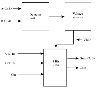 | |
| Fig. 1: | Block diagram of the 8 bit Ripple Carry Adder (RCA) with adaptively controlled VDD |
The virtual VDD is connected to the target 8 bit RCA. Here, P<4:3> are generated in the detector block from A<4:3> and B<4:3>. If both of P<4> and P<3> are high, VDD_high is connected to virtual VDD, because the sum and carry output takes more time to reach the corresponding terminals. If both are low, VDD is connected to VDD_low. Otherwise the sum and carry output reaches the corresponding terminals earlier than that of the previous one. Taking the advantage of this concept, the power dissipation has been reduced drastically by applying adaptive supply voltages. The value of VDD_low is such that the delay of a 8 bit adder with VDD_low is the same as that of the 8 bit adder with VDD_high. Since VDD_low is expected to be much lower than VDD_high, the circuit consumes less power than the conventional method of RCA. Also If P<4> = 1 and P<3> = 0 or If P<4> = 0 and P<3> = 1, the total delay of sum and carry output is equal the delay obtained when VDD =VDD_high.
RESULTS AND DISCUSSION
Analysis of power consumption in adaptive VDD RCA: We analyze the power consumption of the 8 bit Adaptive VDD RCA, using a 0.12 μm CMOS technology with a supply voltage of 1.2 V. The result of analysis makes it possible to optimize the power dissipation and delay.
The total power consumption of the Adaptive VDD RCA is due to three factors.
| F1: | Power consumption of the 8 bit RCA by itself, which is due to portions of the circuit running at |
(F1. a) VDD = VDD_high and
(F1 .b) VDD = VDD_low.
| F2: | Power consumption due to charge/discharge of the virtual VDD node. |
| F3: | Power consumption of the VDD Control circuit. |
Factor F1 accounts for the major portion of the total power consumption. Factor F2 and F3 are the overhead of the proposed approach. Factor F1 is due to the power consumed when VDD = VDD_high and VDD = VDD_low and it depends on the percentage of time the circuit is in the VDD_low and VDD_high mode. Factor F2 is proportional to the frequency of switching between the two supply levels. Since power improvement strongly depends on the percentage of time the circuit is in the VDD_low and VDD_high mode, techniques are needed to put the circuit in the low power mode as much as possible.
Furthermore, to reduce the capacitance of the VDD node, the N-well nodes of all PMOS transistors should be directly connected to the VDD node. Finally, the VDD control circuitry is simple and we can neglect the additional power dissipation due to the control circuitry.
The procedures to evaluate the power consumption due to Factors F1 and F2 are shown as follows.
| S1: | Calculate the critical delay of the 8 bit RCA When VDD =1.2V and P<4:3> = 1. |
| S2: | Calculate the critical delay of the 8 bit RCA When VDD =1.2V and P<4:3> = 0. |
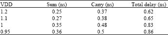
| S3: | Calculate the critical delay of the 8 bit RCA When VDD =1.2V.1.1V, 1V, 0.95V and P<4> = 0, P<3>=1 or P<4>=1, P<3>=0. |
| S4: | Calculate power consumption of the 8 bit adder for VDD=1.2V and P<4:3>=1.Then, calculate that of the other values of VDD. |
| S5: | Calculate power consumption of the 8 bit adder for VDD=1.2V and P<4:3>=0. Then, calculate that of the other values of VDD. |
In both S3 and S4, We assume the input vectors can take random values except bit 3 and 4 because they are fixed to 0 or 1.
The simulation result of Step S1 shows sum delay of 0.34 ns and carry delay of 0.28 ns, so the total delay equal to 0.62 ns for the 8 bit RCA at VDD = 1.2V and P<4:3> = 1. In Step S2, the sum delay of 0.17 ns and carry delay of 0.14 ns, so the total delay is equal to 0.31 ns for the 8 bit RCA at VDD = 1.2V and P<4:3> = 0.
From the results of S1 and S2, we can observe that the sum , carry and total delay of S1 is double than that of S2 when VDD = 1.2V. Also the results of S3 show the total delay of sum and carry at VDD = 1.2V and P<4> = 0,P<3> = 1 or P<4> = 1, P<3> = 0 is equal to the total delay of sum and carry at VDD = 1.2V and P<4:3> = 1. The results of S1 and S2 are shown in Fig. 2 and the results of S3 are shown in Table 1.
Case 1: From Fig. 2 and Table 1, we can conclude that the total delay of sum and carry at various levels of VDD and P<4:3> = 1 is equal to the total delay of sum and carry at different values of VDD and either P<3> = 0, P<4> = 1 or P<3> = 0, P<4> = 1.
Case 2: Also from Fig. 2, we can observed that the total delay of sum and carry equal to the total delay of sum and carry at VDD = 0.95V of case 1.
| Table 1: | Total delay of 8 bit adder unit when either P3 = 0 and P4 = 1 or P3 = 1 and P4 = 0 at different VDD |
 | |
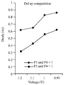 | |
| Fig. 2: | Delay comparison of 8 bit adder unit |
From case 1 and case 2, we identify the values of VDD_low =0.95V and VDD_high = 1.2V.
Then we closely look into the power dissipation of the 8 bit adder unit and it is shown in Fig. 3. Surprisingly, we got the result that the power dissipation of an 8 bit adder unit at different levels of VDD and both P<4:3> = 1 are equal to the power dissipation of an 8 bit adder unit at different levels of VDD and either one of P<3> or P<4> equal to 1 or 0, respectively.
Also from Fig. 3, the power dissipation of an 8 bit adder unit at different values of VDD and both P<4:3> = 1 are slightly higher than other conditions.
So there is power and delay tradeoff occurs in the 8 bit adder unit and we need to get optimized solution for these two factors.
Optimized solution for an 8 bit adder unit: In this research paper, we started with a simple ripple carry adder to show the advantages and effectiveness of the methodology. We can get the optimum solution only by changing the levels of VDD and keeping the delay constant. That means that the delay when P<4:3> = 1 is higher than the delay when P<4:3> = 0 or either <P3> = 1 or <P4> = 0 and vice versa. So we need to check the middle bits <P3> and <P4>. Based on the values of <P3> and <P4>, we adaptively select the supply voltage either VDD_low or VDD_high, because VDD is a far dominant factor for power dissipation as given in Eq. 1.
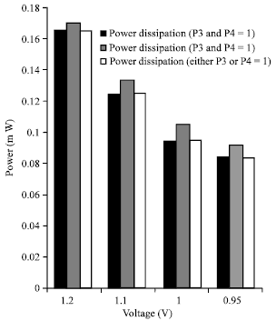 | |
| Fig. 3: | Power dissipation comparison of 8 bit adder unit |
| Table 2: | Summary of proposed work |
The Fig. .2, Fig. 3 and Table 1 show the delay and power dissipation under different set of input vector patterns and at various voltage levels. From which, we can get the optimum solution as the VDD is connected to VDD_low when both P<4:3> = 0. or VDD is connected to VDD_high when both P<4:3> = 1 or either one of P<3> or P<4> equal to 1 or 0, respectively.
From the Table 2, the power dissipation of this proposed work is improved by 80.2%.
CONCLUSIONS
A very low power adder with adaptive supply voltage has been proposed in this research. The proposed method applies a lower supply voltage depending on the input vector patterns to the adder unit. We implemented an 8 bit Ripple Carry Adder (RCA), which shows very low power consumption with comparable performance as a conventional RCA. The proposed 8 bit adder unit shows 80.2% improvements in power consumption with out affecting the other performance like area and delay. It has to be noted that the proposed 8 bit adder unit has the same delay as the 8 bit adder unit designed without applying an adaptive supply voltage.
REFERENCES
- Chandrakasan, A.P., S. Sheng and R.W. Brodersen, 1992. Low power CMOS digital design. IEEE J. Solid-State Circuits, 27: 473-484.
CrossRefDirect Link - Kao, J., M. Miyazaki and A. Chandrakasan, 2002. A 175 MW multiply-accumulate unit using an adaptive supply voltage and body bias architecture. IEEE J. Solid-State Circuits, 37: 1545-1554.
CrossRefDirect Link - Kuroda, T., T. Fujita, S. Mita, T. Nagamatu and S. Yoshioka et al., 1996. A 0.9 V, 150 MHZ, 10 mW, 4 mm 2,2-D Discrete cosine transform core processor with variable threshold-voltage (VT) scheme. IEEE J. Solid-State Circuits, 31: 166-167.
Direct Link - Kuroda, T., K. Suzuki, S. Mita, T. Fujita and F. Yamane, 1998. Variable supply voltage scheme for low power high speed CMOS digital design. IEEE J. Solid-State Circuits, 3: 454-462.
Direct Link - Makino, H., Y. Tsujihashi, K. Nii, C. Morishima, Y. Hayakawa, T. Shimizu and T. Arakawa, 1998. An auto-backgate-controlled MT-CMOS circuit. Proceedings of the Symposium on VLSI Circuits, Jun. 11-13, Honolulu, HI, USA., pp: 42-43.
Direct Link - Vigneswaran, T., B. Mukundhan and P.S. Reddy, 2006. A novel low power and high performance 14 transistor CMOS full adder cell. J. Applied Sci., 6: 1978-1981.
CrossRefDirect Link