
Anwar Sadat
Not Available
Journal of Applied Sciences
Year: 2005 | Volume: 5 | Issue: 8 | Page No.: 1466-1469


ABSTRACT
An interface technique for design and analysis of digital circuit has been devised and described in this study. Basically logic circuits are of two types, one combinational circuit and other is sequential circuit. Logic simulation usually means finding the transient response to a set of time-varying inputs. Simulation follows functional or behavioral level design. Behavioural simulation describes logic function and timing. Functional simulation describes the logic function of a system only but ignores the timing. A simulation program for giving output of digital logic circuits is available now-a-days. But, an approach taken here describes an efficient way to analyze both combinational and sequential circuit. To do this an algorithm has been developed. Finally, a program is coded in Turbo C language and tested for test cases to analyze and give output to that logic circuit.
PDF Abstract XML References Citation
How to cite this article
Anwar Sadat, 2005. A Compiler Driven Simulation Technique for the Analysis of Digital Logic Circuit. Journal of Applied Sciences, 5: 1466-1469.
DOI: 10.3923/jas.2005.1466.1469
URL: https://scialert.net/abstract/?doi=jas.2005.1466.1469
DOI: 10.3923/jas.2005.1466.1469
URL: https://scialert.net/abstract/?doi=jas.2005.1466.1469
INTRODUCTION
Simulation is the process by which a model of the hardware is set up in software or better still, in data structures that are ‘run’ by the software. According to Robert Shanon in System Simulation: the art and science, “Simulation is the process of designing a model of a real system or evaluating various strategies for the operation of the system”. There are two approaches to logic simulation. These are
| • | Event driven |
| • | Compiler driven |
An event driven simulator evaluates a particular element ‘on demand’ only when an input changes. The primary advantage of the event driven simulator is not speed, but timing accuracy. A compiled code simulator evaluates every logical element at every time step regardless of whether there is an input change or not. This type of simulator is designed to check logical correctness at maximum speed. Timing accuracy is regarded as of little importance.
There are several number of simulator developed such as, Parallel multi-delay simulation, SIMLOG, HAL: A High Speed Logic Simulation Machine[1] etc. The Multi-delay Parallel(MDP) technique is a multi-delay logic simulation algorithm that uses no event sorting mechanism. Wide bit-fields and bit-parallel operations are used to resolve out of order events. Although the MDP technique was designed to be implemented in hardware, the software version has proven to be competitive with ordinary multi-delay simulation. There is another logic simulator called SIMLOG[2] which was developed at IIT Kanpur. SIMLOG is written in PASCAL and implemented on the DEC 10/90 as well as IBM PC compatible systems. It has about 1500 lines. It lakes any value of transport delay for an element. It is simpler in the design sense compared to the simulator developed here though a little less efficient.
The compiler driven technique is attempted here for implementation and tested for all sorts of logic circuits. The essence of a compiled code simulator is that the structure of the system being simulated is reflected in the computer store and that each logical element has its own code. Here, timing is ignored and logical correctness alone is checked. A ‘time step’ is considered here which is equivalent to a clock period. Every logical element is evaluated at every time step regardless of whether there is an input change or not. In the case of Sequential circuit it becomes more complex, as any logic gate in the first stage may get input from the next stages. Special arrangements are required to handle this type of feedback. A particular flip-flop is treated here as basic element rather than as devices with feedback. A periodic analysis gives the final stable condition which could be found after several iteration of analysis. The initial state must be known in circuit analysis where logic simulation takes place.
Several key issues of the simulation are the speed of the system and hazard detection. Most systems have some form of limit on the time they take to respond to given conditions. The simulator should be able to detect and report if the timing specifications are violated during operation.
GRAPHICAL ANALYSIS OF DIGITAL CIRCUITS
After the graphical drawing of logic circuits, analysis is done here by compiled code simulation technique. In this technique logical element and the structure of the system being simulated is stored[3] in computer by input description language. Special arrangements are considered to handle feedback.
Input description language: The logic simulator uses a language[4,5] to describe the circuit to be analyzed. This language is textual description, which is more precise than diagrams. Standard hardware description languages such as VHDL[6] are textual. This input description language has all the interconnection information. The description can be hierarchically build up.
In the description of the gates, the first term is the gate name, the second the set of inputs and the third the output. The output name is optional. Where there is more than one input, the set of inputs is enclosed by parentheses.
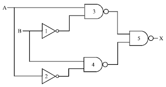
For example, let us take a full adder circuit(Fig. 1). A full adder with inputs A, B and C (carry in) has outputs S (sum) and CO (carry out) defined as:
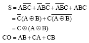 |
Here the symbol ⊕ stands for the exclusive-OR operation.
The input description is as given below:
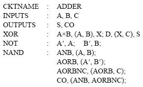 |
Data describing the interconnection of the network must be held in a suitable memory. For each logical element it will be necessary to hold data on inputs and outputs. If a signal is an output of one element and the input of two others, it is recorded only once and has to be modified in only one place when a change occurs. The data structure[7] for storing the various attributes of a gate is discussed here.
| Table 1: | Initial state analysis of exclusive-OR circuit |
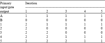 | |
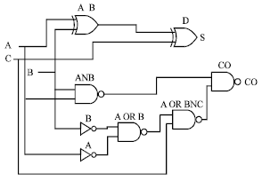 | |
| Fig. 1: | A full adder circuit |
 | |
| Fig. 2: | Exclusive-OR circuit with number for gates |
At first, each gate is described by the following quantities:
| • | Name |
| • | Index I |
| • | Output value |
| • | NFO-Number of fanouts |
| • | NFI-Number of fanins |
| • | FOL-Pointer to a list called IOLST. FOL points to first fanout. Next (NFO(i) - 1) locations of IOLST contain remaining fanouts of I. |
| • | FIL-Pointer to IOLST. Similar to FOL but for inputs. |
| • | Type (NAND, NOR, etc.) |
| • | Delay |
INITIAL STATE ANALYSIS
Logic simulation usually means finding the transient response to a set of time-varying inputs[4,8].
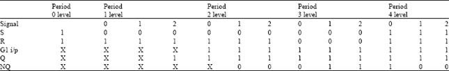
| Table 2: | Simulation of R-S flip-flop circuit |
 | |
 | |
| Fig. 3a: | R-S flip-flop |
 | |
| Fig. 3b: | R-S flip-flop with feedback broken |
In the simplest case, these inputs switch back and forth between 0 and 1 at specified times. Output variations, again between 0 and 1, are to be found as a function of time. Logic simulation is usually preceded by an initial state analysis. Outputs of all elements are found at t = 0. Memory elements like NAND or NOR latches, must have this initial state specified.
Considering the exclusive-OR circuit shown in Fig. 2. Let us assume the initial inputs to be A = 1, B = 0. It is necessary to find the outputs of all gates at t = 0. This is done in several iterations. In the first iteration no gate output is known. All unknown outputs are indicated by iteration 2. In each iteration, the output of a gate is found by taking input values from the previous iteration. Initial state analysis is completed when all outputs are found and when two successive iterations give the same values. Results for the exclusive-OR circuit are given in Table 1. Iterations 4 and 5 give the same output values and we stop after iteration 5.
HANDLING FEEDBACK
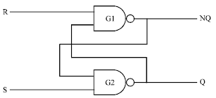
One problem that has to be solved is feedback loops within logic. As the feed back signals effectively provide second or possibly further input vectors for each vector of the primary inputs, the circuit behaviour becomes difficult to predict. Consider the simple R-S flip-flop shown in Fig. 3a.
 | |
| Fig. 4: | Flowchart for a logic simulator |
The signals R and S are both level 0. G1 is at a level one greater than the level of G2 is at a level one greater than the level of G1 output. This is a deadlock situation.
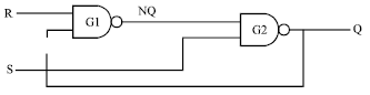
The way to deal with t his is to break the feedback loop[4]. Suppose that the second input of G1 is disconnected from Q and treated as a primary input at level 0 and with unknown logic value. The feedback loop is now broken as shown is Fig. 3b. When the circuit is simulated, G1 is evaluated at level 1 and subsequently G2 at level 2. Table 2 shows such an evaluation. S and R start at 1 and Q and NQ are unknown, X. Primary inputs are shown bold.
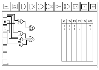 | |
| Fig. 5: | Developed software for the digital circuit drawing and analysis |
Suppose S now goes to 0. Level 1 is not affected, but at level 2, Q is forced to 1. As the feedback loop is broken, nothing further occurs. However, note that the inputs to G1 are now known, so further simulation should take place. Thus the feedback signal is a level 0 signal. Another cycle of simulation takes place causing NQ to become 0 in level 1. There are no changes at level 2. The simulation takes place.
In Table 2, period 3 shows what happens when R goes to 0. NQ is forced to 1 at level 1 and, as S is already 0, Q remains at 1, so there is no change at level 2. Again, the simulation takes place.
In period 4, R and S both return to 1 at he same time. At level 1 NQ is driven to 0. This zero causes Q to remain at 1 in level 2. This will always be the case with this simulator. However, in a real circuit it is not known which state the flip-flop would assume. Whenever the simulator encounters this sort of ambiguous situation it warns the user and this is a feature of this software.
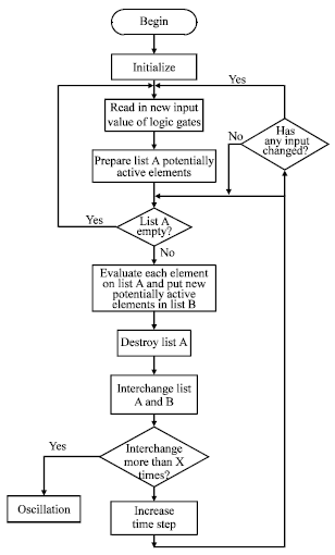
FLOWCHART OF THE LOGIC SIMULATOR
Figure 4 shows gives the flow chart for the logic simulator using selective trace. It is assumed that no new input will change till the circuit has stabilized after previous input changes. Therefore, one check for input changes only after list B becomes empty. If the circuit does not stabilize after a given number of time steps, it is assumed that there are oscillations. Oscillations are detected if lists A and B are exchanged more than a given number of times (e.g. four times).
CONCLUSIONS
The design and output screen of the developed software is given in the Fig. 5. The screen shows the output result[9] of a full adder circuit for a particular input combination. The logic simulator developed here is efficient and simple. Compiler driven technique is used to analyze the logic level of both combinational and sequential logic circuit. Emphasis is given on a gate level simulation. Special arrangements were done to detect and handle the feedback of the sequential circuit, which are more complex. Steps were taken to find out the initial state and final stable condition of a gate. Here, the execution speed can be considerably improved by selectively analyzing only those gates, which lie on the signal flow path. There are some scopes to enhance the speed of the system. Timing information can be obtained by assigning different delays to different gates. There are scopes for further improving the simulator’s behaviour of real electronics June 15, 2005 using event driven simulation technique.