
N. Siva Sankara Reddy
Department of Electronics and Communication Engineering, Vasavi College of Engineering, Ibrahimbagh, Hyderabad-500031, India
Asian Journal of Applied Sciences
Year: 2011 | Volume: 4 | Issue: 6 | Page No.: 657-662


ABSTRACT
The need for low power and high efficiency electronics is felt more and more with the proliferation of complex mobile gadgets into our daily use. This paper describes about implementation of low power techniques to different designs using VERILOG HDL (Hardware Description Language) through simulation and synthesis and finally implement some of the low power techniques in the design of 16 bit CPU. The power reports after synthesis indicate that there is about 29% of power saving in the 16 bit processor when these low power techniques are applied.
PDF Abstract XML References Citation
Received: March 01, 2011;
Accepted: April 20, 2011;
Published: June 29, 2011
How to cite this article
N. Siva Sankara Reddy, 2011. Minimization of Power Dissipation in 16 Bit Processor using Low Power Tecniques. Asian Journal of Applied Sciences, 4: 657-662.
DOI: 10.3923/ajaps.2011.657.662
URL: https://scialert.net/abstract/?doi=ajaps.2011.657.662
DOI: 10.3923/ajaps.2011.657.662
URL: https://scialert.net/abstract/?doi=ajaps.2011.657.662
INTRODUCTION
In all the battery operated devices, there is a need to reduce power dissipation to avoid frequent recharging and thereby increase battery life, reduce the size of battery and cooling system needed for removing the heat. So it is necessary to reduce the power dissipation in IC’s. Power dissipation can be minimized at various levels like system level, behavioral level, architectural level, circuit level, physical design and technology level. There is considerable effort put in, through out the world, to reduce power dissipation in VLSI circuits, to increase the life of the battery and to prevent hot spots. There are several approaches suggested. Siva Sankara Reddy et al. (2008) described glitch free and cascadable logic to reduce power dissipation using adiabatic logic. Vigneswaran and Reddy (2006) have described low power 8 bit adder unit with adaptive supply voltage. Vijayakumar et al. (2007) explained about optimizing CMOS circuits for performance improvements using adiabatic logic. Vigneswaran et al. (2006) have described about low power and high performance 14 transistor CMOS full adder cell. Islam et al. (2009) have explained about Low cost quantum realization of reversible multiplier circuit. Chandrakasan et al. (1992) have described about techniques for Low-Power CMOS Digital Design. Lin and Tsai (2002) have described about theoretical Analysis of Bus-Invert Coding which consists of calculation of hamming distance in theoretical approach and also the effect of transitions on the bus. Liu and Svensson (1994) have described about Power consumption estimation in CMOS VLSI chips. Paul et al. (2006) have described about Low power design techniques for scaled technologies. Benini and De Micheli (1994) have described about State Assignment for Low-Power Dissipation.
In this study, we have described about application of various low power techniques using verilog hardware description language through simulation and synthesis. The various low power techniques are given below.
LOW POWER TECHNIQUES
The different low power techniques used in our designs are (1) State machine encoding (2) Resource sharing (3) Register retiming (4) Operation substitution (5) Operation reduction (6) Bus invert coding (7) Minimizing data transitions on bus (8) Clock gating (9) Reduced supply voltages (10) Resizing of the transistors (11) Reducing power dissipation in dynamic memories.
Gray encoding consumes lesser power as compared to binary encoding because gray encodings have only a single bit change while going from one state to another so that number of transitions is reduced i.e. switching activity is reduced so that power is reduced. Any logic element will contribute to power consumption as it has a capacitance attached to it and transitioning of data through that logic will lead to power dissipation. Resource sharing is an optimization technique that uses a single functional block (such as an adder or comparator) to implement several operators in the HDL code. Register retiming is a concept mostly used in improving timing by reordering the combinational and sequential logic in a given data path. In certain cases, there is a saving of logic and thus can help improve upon power consumption.
Certain operations require more computational energy than others. Replacing multiplication by addition can not only save area but also achieve improvement in power dissipation so that energy per consumption is reduced but this is achieved at the cost of small increase in delay. Reducing the operations count reduces the total capacitance associated during that operation and hence can reduce power dissipation.
Bus invert coding is a technique in which if the hamming distance between the current data and the next data is more than N/2 (where N is the bus width), then one can invert the bits and send it to the receiving end, so as to minimize the number of transitions on the bus. In that case, a control bit goes along with the data to indicate the receiving end, whether the data is inverted or not. Whenever, transmission of data on the data buses has been completed and if there is no valid data applied to the data bus, the general practice is to reset the data bus until the next valid data is applied. Instead of this we can store the latest arrived data for data buses so that there is a probability for reducing the switching activities when the next data is applied.
In many instances, data is loaded into register infrequently but the clock signal continues to switch at every clock cycle. Sometimes registers are assigned the same value for every clock cycle. To prevent clock from triggering the registers, a gating circuit can be used to shut off the clock from these circuits. By reducing the quiescent current of operation and operating the circuit at lower voltages, we can reduce the power dissipation in the circuits. However, when the supply voltage is reduced there will be increase in delay.
When the size of the transistor is reduced, the resistance increases and the current flowing through it decreases. Hence the power dissipation will be reduced due to the reduced current of operation. However, if the transistor size is reduced to below a certain limit, the delays will increase. In case of dynamic memories the data will be stored by charging or discharging the capacitance through bit line and controlling the operation using word lines. In this technique by reducing the voltage and increasing the capacitance we can save some power.
Design of 16 bit cpu using low power techniques: A 16 bit processor has been designed using some of the low power techniques discussed above. The block diagram of the 16 bit CPU (central processing unit) is shown in Fig. 1. The processor contains number of blocks which include a register array of eight bit registers, an ALU (Arithmetic Logic Unit), a shifter, a program counter, an instruction register, a comparator, an address register and a control unit. All these units communicate through a common 16 bit tri-state bus.
There are different types of Instructions for CPU. Load instructions are used to load register values from other registers, memory locations or with intermediate values given in instruction.
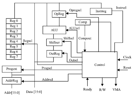 | |
| Fig. 1: | Block diagram of 16 bit CPU |
ALU instructions perform arithmetic and logical operations such as ADD, SUBRACT, Bitwise OR and NOT, XOR, XNOR, Reduction AND, Reduction OR, Reduction XOR, Reduction XNOR, Logical AND or etc. Shift instructions use the shift unit to perform shift operations of the data passed on to it such as shift left, shift right, rotate left, rotate right, arithmetic shift left, arithmetic shift right. Compare instructions use the compare unit to perform compare operations on to the data passed on to it such as equal to, not equal to, greater than, greater than equal to, less than, less than equal to etc. There are different opcodes for different operations. For example, 00010 is the opcode for adding two different register values.
RESULTS AND DISCUSSION
All the blocks of CPU have been designed using verilog hardware description language. The various modules of CPU are program counter, regarray module, trireg module, ALU module, shift register module, comparator module, control unit module, memory module etc. The names of various signals of CPU block we have used are clock, reset, ready, rw, vma, data, progcntrwr, addr, aluout, alusel, inc, shiftout, shiftsel, compsel, compout etc. In each module, there are different types of inputs and outputs. For example, the ALU module has 3 inputs and an output. Depending on alusel line, the corresponding alu operation is performed on data inputs sent and puts data on the output aluout.
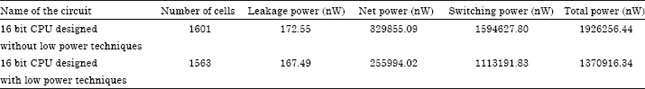
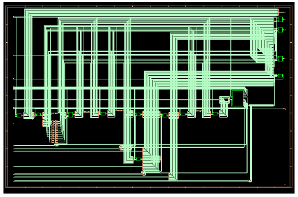
The simulation of 16 bit CPU has been performed using Cadence Tool NC-Verilog and the functionality is verified for different instructions. Typical simulation waveforms for add instruction are shown in Fig. 2. In Fig. 2, clock, reset are the single bit inputs, addrregwr, inc are the 1 bit inouts, data, opdata, aluout, addr are 16 bit inouts, alusel is 5 bit inout. The synthesis of 16 bit CPU has been performed for both ASIC and FPGA implementations. The power report results of CPU without and with low power techniques generated by cadence tools after synthesis are shown in Table 1. From the simulation results, the functionality of 16 bit CPU has been verified and from the power reports, it is observed that there is power saving of about 29% in the CPU designed with low power techniques when compared to the CPU designed without these low power techniques. The RTL schematic of CPU designed with Low power techniques is shown in Fig. 3. The cell layout generated by SOC encounter for this CPU is shown in Fig. 4. The 16 bit CPU has been downloaded onto FPGA and typical results of chip scope pro after downloading the CPU onto FPGA for ADD instruction are shown in Fig. 5.
| Table 1: | Power report results after synthesis |
 | |
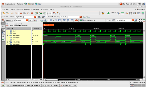 | |
| Fig. 2: | Simulation waveforms for ADD instruction |
 | |
| Fig. 3: | RTL schematic of CPU with low power techniques |
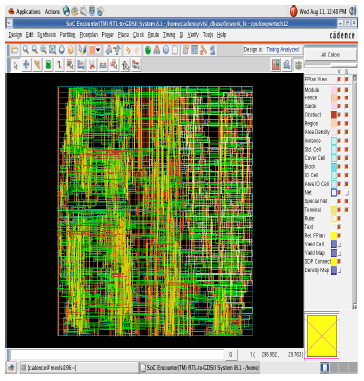 | |
| Fig. 4: | Cell layout generated by SOC encounter for the CPU designed with low power techniques |
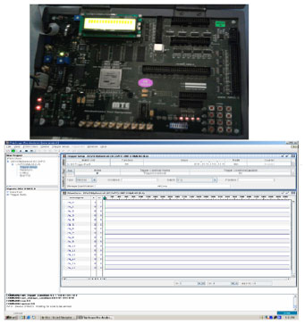 | |
| Fig. 5: | Snapshot of FPGA and Chip scope results for ADD instruction after downloading onto FPGA |
CONCLUSION
This study reports several approaches through simulation and synthesis which can reduce power dissipation in VLSI circuits. The design styles mentioned in this study have a significant impact on the overall power consumption of the circuits and they do not affect the functionality of the designs. A 16 bit CPU has been designed by using the low power techniques and it is simulated and synthesized, cell layout generated and downloaded onto FPGA. From the synthesis results, it is observed that there is power saving of about 29% when these low power techniques are applied in the CPU designed when compared to the power dissipation of the CPU designed without these low power techniques.
ACKNOWLEDGMENT
I would like to thank Prof P.A. Govindacharyulu for the discussions I had from time to time.
REFERENCES
- Reddy, N.S.S., M. Satyam and K.L. Kishore, 2008. Glitch free and cascadable adiabatic logic for low power applications. Asian J. Scientific Res., 1: 464-469.
CrossRefDirect Link - Vigneswaran, T. and P.S. Reddy, 2006. A novel low power 8 bit adder unit with adaptive supply voltage. J. Applied Sci., 6: 2936-2939.
CrossRefDirect Link - Vijayakumar, P., M. Shanthanalakshmi and K. Gunavathi, 2007. Optimizing CMOS circuits for performance improvements using adiabatic logic. Inform. Technol. J., 6: 325-331.
CrossRefDirect Link - Vigneswaran, T., B. Mukundhan and P.S. Reddy, 2006. A novel low power and high performance 14 transistor CMOS full adder cell. J. Applied Sci., 6: 1978-1981.
CrossRefDirect Link - Islam, M.S., M.M. Rahman, Z. Begum and M.Z. Hafiz, 2009. Low cost quantum realization of reversible multiplier circuit. Inform. Technol. J., 8: 208-213.
CrossRefDirect Link - Chandrakasan, A.P., S. Sheng and R.W. Brodersen, 1992. Low power CMOS digital design. IEEE J. Solid-State Circuits, 27: 473-484.
CrossRefDirect Link - Lin, R.B., and C.M. Tsai, 2002. Theoretical analysis of bus-invert coding. IEEE Trans. Very Large Scale Integr., 10: 929-934.
Direct Link - Liu, D. and C. Svensson, 1994. Power consumption estimation in CMOS VLSI chips. IEEE J. Solid State Circuits, 29: 663-670.
Direct Link - Paul, B.C., A. Agarwal and K. Roy, 2006. Low power design techniques for scaled technologies. Integr. VLSI J., 2: 64-89.
CrossRef