
A. Peiravi
Department of Electrical Engineering, School of Engineering, Ferdowsi University of Mashhad, Mashhad, Iran
Journal of Applied Sciences
Year: 2008 | Volume: 8 | Issue: 24 | Page No.: 4570-4578


ABSTRACT
In this study, a software technique for the design of combinational digital circuits with minimum silicon surface allocation and gate propagation delay using genetic algorithm is presented. In existing methods which use the initial chromosome for the gate and then find the optimum solution using a library of gates, there is a possibility of missing some possible combinations of primary circuits with which the desired function may be realized. Thus, the outcome may be a local optimum, not the global one. In our approach to this problem, all the possible states of a circuit are first analyzed. The program will automatically define the initial chromosome and proceed to find the optimum circuit for the desired function. The program has been coded in C++ and it includes a library of the various gates with their respective size on the silicon wafer and propagation delay.
PDF Abstract XML References Citation
How to cite this article
A. Peiravi, 2008. A Genetic Approach to the Synthesis of Combinational Circuits with Optimum Area and Speed. Journal of Applied Sciences, 8: 4570-4578.
DOI: 10.3923/jas.2008.4570.4578
URL: https://scialert.net/abstract/?doi=jas.2008.4570.4578
DOI: 10.3923/jas.2008.4570.4578
URL: https://scialert.net/abstract/?doi=jas.2008.4570.4578
INTRODUCTION
There has been considerable use of genetic algorithms in the various aspects of design of VLSI circuits and systems. Many researchers have presented various applications of genetic algorithms. One may name automatic test generation as a specific application. For example, Sabry et al. (1998) presented a new technique for test pattern generation based on a genetic algorithm and parallel processing techniques. Their method offered compact test sets, compared to other methods that achieve maximum coverage.
What is usually important in the design of VLSI circuits is area consumption on the silicon chip and the circuit speed or its propagation delay. Moreover, optimum design of floorplannig in the layout design of VLSI circuits is another application. Floorplanning of VLSI design is a key design flows which determines chip size, electrical characteristics, timing constrains, etc. of the final silicon chip. Many useful floorplan tools are available which provide user-friendly interactive environments with useful information for chip design. However, construction and decision-making of floorplan design itself relies on the insight of human beings. Therefore, the results depend on the person who uses the tool and the initial conditions. Maurizio and Matteo (1996) presented a genetic algorithm to optimize floorplan area based on suitable techniques for solution encoding and evaluation function definition, effective cross-over and mutation operators and heuristic operators. Their adaptive approach automatically provided the optimal values for the activation probabilities of the operators. Experimental results showed that their proposed method is competitive with the most effective ones as far as the CPU time requirements and the result accuracy is considered. Moreover, it required a limited amount of memory. Eguchi et al. (1998) proposed application of genetic algorithms to floorplanning for the purpose of providing better initial conditions as a starting point of design work to novice designers. They discussed a floorplan placement model suitable to Genetic Algorithms and carried out some computational experiments to show practical possibility. Circuit synthesis of a given function is another possible application since power dissipation is becoming a limiting factor in the realization of VLSI systems due to maximum operating temperatures and battery life constraints in the ever-increasing portable applications. Digital Signal Processing (DSP) applications are relatively complex. Therefore, their power dissipation is of special significance and low-power design techniques are emerging which vary depending on the level of the design that they target, ranging from the semiconductor technology to the higher algorithmic level. Arslan et al. (1996) used genetic algorithms for synthesis of low power digital signal processing circuits. They described two different techniques which employed genetic algorithms for synthesis of digital circuits. Their first technique employed a multi-objective genetic algorithm for synthesizing low power circuits. A gate-level description of the circuit is encoded into a single chromosome and the genetic algorithm evolves by searching for circuit structures that are optimized for both overall capacitive area and critical path which would allow operation under reduced power supply voltages. Their second technique operated on a Data Flow Graph (DFG) consisting of high level blocks such as registers, adders and multipliers. Operations such as retiming and automatic pipelining were used to reduce the critical path of the DFG, hence allowing operation under reduced supply voltage. Bright and Arslan (1996) presented a technique for optimizing CMOS based DSP systems for power. They used a genetic algorithm to reduce power, while tracking area and speed specifications, through the application of high level transformations. Their algorithm searches for systems with the lowest power consumption within a large solution space. They showed that the genetic algorithm is an efficient tool for optimizing power consumption in the design of complex VLSI systems. Other researchers have used other techniques for similar goals. For example, Raja et al. (2004) used linear programming to design CMOS circuits with minimum dynamic power and highest speed, i.e., least delay. Present experience has shown that optimal design using genetic algorithm is able to provide us with the optimum circuit design for both area consumption and speed for a given desired function. Reis et al. (2003) proposed a genetic algorithm for designing combinational logic circuits. They studied four cases with the objective of generating a functional circuit with the minimum number of gates. Reis et al. (2007) presented an analysis of the performance of a genetic algorithm in the synthesis of digital circuits using two approaches. Their first concept was to improve the static fitness function by including a discontinuity evaluation and their second concept was to extend the static fitness by introducing a fractional-order dynamical evaluation. In this study, the results of applying genetic algorithms for the optimal design of combinational circuits in terms of both surface area of silicon and speed are presented. The technique presented here can be extended to the optimal synthesis of sequential circuits and even more sophisticated digital applications. The general approach is to encode a chromosome with the inputs and outputs of the gates and genetic operations are carried out on the chromosomes until the optimal solution is obtained.
EXISTING GENETIC APPROACH
Arslan et al. (1996) used genetic algorithm for the synthesis of digital circuits. Their main objective was to minimize power consumption. They presented details on how they defined a chromosome to incorporate the attributes of digital circuits. For example, you can see how the circuit shown in Fig. 1 is coded into a chromosome.
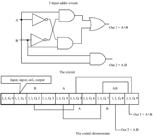 | |
| Fig. 1: | A two input adder circuit and the corresponding chromosome |
 | |
| Fig. 2: | A starting population of chromosomes |
 | |
| Fig. 3: | An example fitness function to be used for the above population |
 | |
| Fig. 4: | The roulette wheel selection method proportional to fitness |
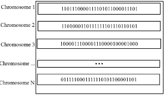
This way, they defined a chromosome and generated others which make up the starting population as shown in Fig. 2. Some of the existing genes such as those related to the input-output of the circuit are constant in all chromosomes. However, other parts on which the various genetic operators function are different in various chromosomes.
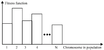
They started out with this starting population each of which indicates a possible solution to the problem at hand. Then a fitness function such as shown in Fig. 3 is used to evaluate the fitness of each chromosome in the starting population.
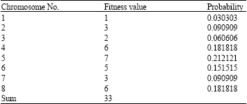
| Table 1: | Roulette wheel probability according to fitness value |
 | |
This fitness function should be defined in such a way that it helps identify the optimal solution.
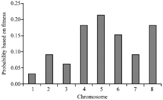
Defining the starting population and the fitness function are the preparatory steps of a genetic algorithm. This population must reproduce to start the algorithm. At first the best chromosomes are chosen using the fitness function to be used in the reproduction cycle. Three methods that are usually used for this selection are roulette wheel (Table 1), rank selection and tournament as shown in Fig. 4-6.
Since the roulette wheel selection method gives the probability of selection proportional with the fitness of the chromosomes, even the weak chromosomes have some chance of selection. Even the weak chromosomes may have genes with positive qualities which may be useful in the latter generations, this selection method is used in this research. The next step of the algorithm would be crossover and mutation which are used to generate the next population. Two forms of crossover operation are shown in Fig. 7 and a circuit level description of the crossover operation is shown in Fig. 8.
In the mutation operation, some of the bits (or digits) which make up a given chromosome are changed at random. An example of mutation is shown in Fig. 9. Usually a very low probability is used for the operation of mutation on the chromosomes.
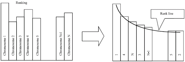 | |
| Fig. 5: | Ranking selection method |
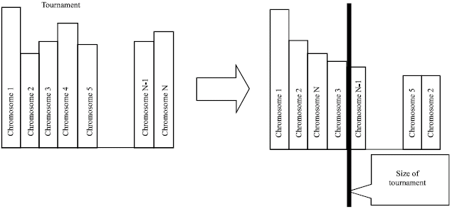 | |
| Fig. 6: | Tournament selection method |
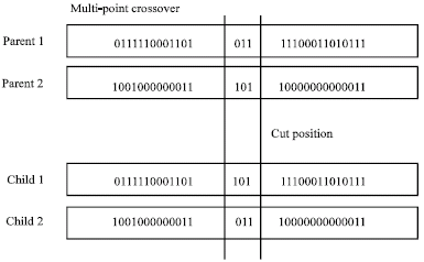 | |
| Fig. 7: | Two forms of crossover operation |
Then the best chromosome in the new population is determined using the fitness function and the procedure is repeated again until the optimal solution is found using a predefined limit for the fitness function as a criteria as shown in Fig. 10.
 | |
| Fig. 8: | A circuit level crossover operation |
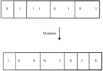 |
| Fig. 9: | Mutation operation |
Gate delay and total area: The speed of operation of a VLSI circuit depends on the technology used, the size of the transistors in the circuit and the circuit topology and structure. For example, the normalized delay of several gates in 2 micron technology is shown in Fig. 11.
Gate delay consists of an electrical and a parasitic component. The resistance of the interconnects and the capacitive effects of the source drain regions may be modeled as an RC circuit to compute the gate delay.
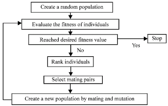 | |
| Fig. 10: | The usual flow of operations in a genetic algorithm |
| Table 2: | Gate delay for a few CMOS gates |
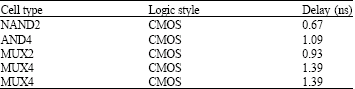 | |
Typical values of gate delay for several gates are shown in Table 2 as an example.
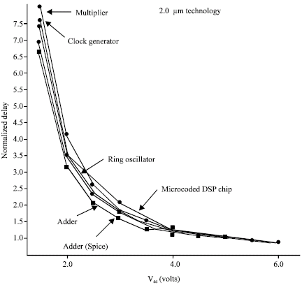 | |
| Fig. 11: | Normalized delay for several gates in 2 micron technology |
| Table 3: | Library of gates |
 | |
The numbers shown in Table 2 are not exact and their true value depends on the technology scale and the exact specifications of the gate.
The total area used by a given circuit is the total size of the transistors, their interconnections and the spacing required by the design rules.
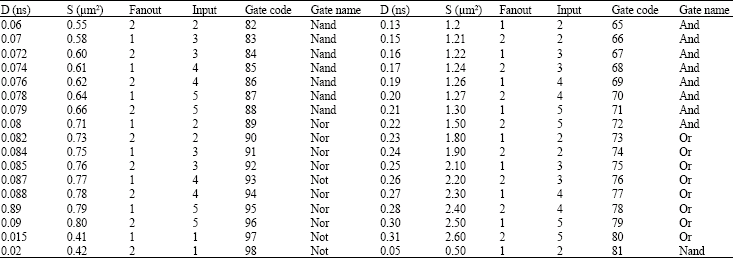
Coding a chromosome: A circuit must be converted into a sequence of digits which indicate its behavior, structure and physical characteristics in order to generate the initial chromosome. The behavioral section shows the inputs and the outputs. The structural part shows the type of gate used such as an AND gate, an OR gate or a NOR gate and their interconnection. The physical characteristics part shows circuit qualities of interest such as die area consumption and propagation delay. These characteristics are shown in Table 3 for gates used in CMOS technology where, S denotes the area and D denotes the delay of the gate.
The chromosome of a given logic circuit would have several sections each of which is related to the coding of the gate that it is made of. Each gate is described by a sequence of digits made up of nine pairs as shown in Table 4.
For example, the logic circuit shown in Fig. 12 below is coded into the following chromosome:
| Table 4: | Coding a gate into a sequence of digits |
 | |
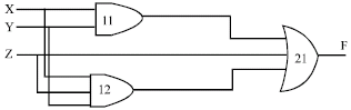 | |
| Fig. 12: | A sample logic circuit with three inputs and one output |
The chromosome for the gates in the above circuit are as follows:
| 1-A two input AND gate |
| 116601020000002100 |
| 2-A three input AND gate |
| 126701020300002100 |
| 3-A three input OR gate |
| 217511120300001000 |
The overall chromosome is the sequence of the above three.
Forming the population: The program developed uses this chromosome and generates the starting population considering the number of gates and the input and output of the circuit.
Fitness of the initial chromosomes: The most important part of the genetic algorithm is the fitness function. Arslan et al. (1996) who aimed at minimizing power consumption used the following flowchart in order to process the chromosomes in their genetic algorithm as shown in Fig. 13.
What is important here is that they aimed at minimizing power consumption, while we intend to find the best circuit with minimum die area consumption and delay. The procedure starts out with a target logic function which is to be synthesized. The chromosomes in the starting population are processed and then their functional fitness, delay fitness and area fitness is evaluated. The fitness function is defined as a three part function each of which is used for evaluating one of the characteristics of the generated circuit. The first part checks for the validity of the generated function for each chromosome and allocates a score to it. The second part calculates the total silicon area consumption and allocates a score to the chromosome.
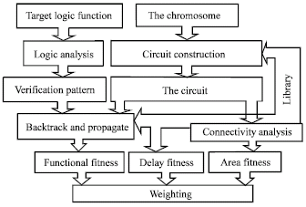 | |
| Fig. 13: | The various parts of the fitness function |
The third part calculates the propagation delay in the circuit as the sum of the delays of the longest path from the input to the output and allocates a score to the chromosome.
In present approach, to calculate the function fitness for the initial chromosomes, the truth table of that chromosome is tested by applying the inputs and checking the output with the desired output. Each instance of correspondence with the desired output is given a value of one and each instance of not corresponding with the desired output is given a value of zero. Thus the overall fitness of the initial chromosome is calculated from the following equation:
where, Foi is one whenever the output of the circuit matches the desired output and is zero whenever it does not match. Obviously n is the number of rows in the truth table and the value of t is always somewhere between 0 and 10.
To calculate the fitness of the chromosome in terms of delay, the delay of the path with the longest delay between the inputs and the output of the circuit is found by using the delays of the gates in the library. This value is also always between 0 and 10.
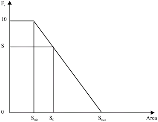
As far as silicon area used is concerned, the circuit is more fit if the total area used by the gates in it is less. The part of the fitness function related to surface area consumption of the circuit is calculated from the following equation which is also demonstrated in Fig. 14:
 | |
| Fig. 14: | Fitness function for die surface area consumption of the circuit |
 | |
| Fig. 15: | Fitness function for delay of the circuit |
where, Smax equals the upper limit of the No. of gates times the area of the gate with the maximum surface area in the table, Smin is the lower limit of the No. of gates times the area of the gate with the minimum area and Sc is the silicon die area for the circuit in the chromosome. A circuit with Smax would then have a fitness value of 0, while, a circuit with Smin would have a fitness value of 10.
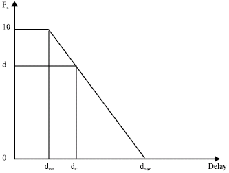
As far as delay is concerned, the circuit is more fit if the total delay used by the gates in it is less. The part of the fitness function related to delay of the circuit is calculated from the following equation which is also demonstrated in Fig. 15:
where, d is the delay of the critical path of the chromosome, dmax is set to be six times the highest delay in the available gates since a maximum of five stages of gates are assumed in our synthesis and dmin is the delay of the gate with the minimum delay in the library of gates assuming a minimum of one stage for the realization of a given function.
Thus, the overall circuit fitness may be computed using the above three criteria by using the following overall fitness function that is used for the circuit:
where, the coefficients may be chosen based on the importance of each factor which makes up the fitness function. In this function, t denotes the function fitness, d denotes the delay fitness value and s denotes the silicon consumption fitness value. Each of these values are chosen between 0 and 10, but may be changed depending on how we value the optimality of each factor.
Since we cannot find the smallest gate with the least delay at the same time, this combined fitness function may be used to enable the designer to make a trade-off between optimum size and speed. The value of t is always set to ten for chromosomes which are suitable for the realization of the desired function and set to 0 otherwise. The coefficient used for t in the fitness function can be used to place more or less importance on this factor compared to optimality for size and speed. The values mostly used in this research were ten for A, two for B and one for C. However, any other combination of these coefficients may be used. Once the fitness value of the chromosomes in the initial population is calculated, some chromosomes should be selected using crossover and mutation operations. The Roulette wheel approach is used for the selection of chromosomes in this research where, the probability of selection is proportional with the fitness of each member. Therefore, an upper bound and a lower bound for their fitness for the circuit are computed. We generate a random number based on which the chromosome is selected. The number of chromosomes is predetermined based on the size of the population. The selected chromosomes are ordered as they are selected. Two crossover operators act on each chromosome. If the number of the gates in the chromosome is assumed to be n, one of the gates in the chromosome is selected with the probability of 1/n. Since each gate consists of four sections, one section of the gate is selected with a probability of 0.25 and it is crossovered with the same section of another gate producing two new chromosomes. The number of chromosome pairs on which the crossover operator is performed is controlled by an input from the program. Many states may be generated as a result of the crossover operator which are not acceptable at all. For example, there may be too many outputs, two few inputs or even a sequential circuit may be generated. To reduce the chances of such chromosomes from being selected in the next generations, their function fitness value is set equal to zero and only their area consumption is computed. Mutation is carried out in the next step on selected chromosomes based on a predefined percentage which is input by the operator. A percentage of the chromosomes is thus selected using a roulette wheel and mutation is done on predefined sections at random. Again the function fitness for instances which are not acceptable such as having loose internal connections, or being sequential in nature are set to zero to reduce the chances of such chromosomes from being selected in the next generations. Next, the elitism operation is performed on the resulting chromosomes. The most elite chromosomes are selected and they form the next generation. This procedure is repeated until the fittest chromosome is found based on a predefined lower bound input by the operator.
RESULTS AND CONCLUSIONS
The code has been developed in Borland C++ Builder 6 and ran on an IBM personal computer with the following bounds imposed on the genetic operators:
The maximum value for the fitness function is 130 using A = 10, B = 2 and C = 1. Therefore, the least value that a suitable circuit which could satisfy the desired function could have was 100 and the maximum value that an unsuitable circuit which could not satisfy the desired function could have was 30. Thereby, unsuitable chromosomes would be eliminated rapidly as the new generations evolved. Present experience with this software showed that for many circuit synthesis examples which we ran, the results approached the optimal design after 100 or more generations had evolved and the fitness value exceeded 127.
The details of a genetic approach to the synthesis of combinational circuits has been presented here and it is shown that this approach can lead to the synthesis of circuits with optimum silicon area consumption and minimum delay in a very short time. Present approach is superior to existing synthesis approaches where, a predefined algorithm is used to generate the circuit. Present approach gives a wider selection possibility and yields optimum circuits for the realization of the desired function. The program developed is easy to use and can be extended to cover the optimal synthesis of analog and more sophisticated digital circuits if the necessary funding for its extension is provided.
ACKNOWLEDGMENT
I would like to thank Mr. F.B. Bajgiran for his assistance in this study.
REFERENCES
- Sabry, M., A. Wahba and H. Mahdi, 1998. A parallel technique for ATPG using genetic algorithms. Proceeding of the 10th International Conference on Microelectr, December 14-16, 1998, Tunisia, pp:71-74.
CrossRef - Eguchi, K., J. Suzuki, S. Yamane and K. Oshima, 1998. An application of genetic algorithms to floorplanning of VLSI. Proceeding of the 1st International Conference Rough Sets Current Trends Computer, January 1, 1998, Springer-Verlag, pp: 263-270.
CrossRefDirect Link - Arslan, T., E.E. Ozdemir, M.S. Bright and D.H. Horrocks, 1996. Genetic synthesis techniques for low-power digital signal processing circuits. Proceeding of the Colloquium Digital Synthesis, February 15, 1996, London, UK., pp: 7/1-pp: 7/5.
Direct Link - Maurizio, R. and S.R. Matteo, 1996. GALLO: A genetic algorithm for floorplan optimization. Proceedings of the Transactions on Computer-Aided Design Integrated Circuits and System, Volume 15, August 6, 1996, IEEE Xplore Pub., pp: 943-951.
CrossRefDirect Link - Reis, C. and J.A.T. Machado, 2003. An evolutionary approach to the synthesis of combinational circuits. Proceedings of the International Conference on Computational Cybernetics, August 29-30, 2003, Siofok, Hungry, pp: 1-6.
Direct Link - Bright, M.S. and T. Arslan, 1996. A genetic framework for the high-level optimisation of low power VLSI DSP systems. IEE Elect. Lett., 32: 1150-1151.
Direct Link - Reis, C., J.A.T. Machado and J.B. Cunha, 2007. A Fractional Calculus Perspective in the Evolutionary Design of Combinational Circuits. In: Advances Fractional Calculus, Part 5, Sabatier, J., O.P. Agrawal and J.A. Tenreiro Machado (Eds.). Springer, Netherlands, ISBN: 978-1-4020-6041-0 pp: 305-322.
CrossRef