
M. Djavid
Department of Electrical Engineering, K.N. Toosi University of Technology, Tehran, Iran
A. Ghaffari
Department of Electrical Engineering, K.N. Toosi University of Technology, Tehran, Iran
F. Monifi
Department of Electrical Engineering, K.N. Toosi University of Technology, Tehran, Iran
M.S. Abrishamian
Department of Electrical Engineering, K.N. Toosi University of Technology, Tehran, Iran
Journal of Applied Sciences
Year: 2008 | Volume: 8 | Issue: 10 | Page No.: 1891-1897


ABSTRACT
In this study, we propose a new type of photonic crystal band-pass and band-stop filter based on biperiodic structure. Usually two types of photonic crystal band-pass filters are utilized in optical circuit. In the first one Fabry-Perot cavities are used while in the second one cavity-coupled waveguide are used. We optimize the second structure in this study. Then we show that by little changing in the band-pass structure, a band-stop filter is attained. Using Finite-Difference Time-Domain (FDTD) method we achieve output efficiency over 98% for band-pass filter and below 3% for band-stop filter. Also we investigate filter tunability parameters which affecting central frequency of these filters. Further analysis shows that the central frequency of transmission band (stop band) can be changed by altering the refractive index of bigger rods in biperiodic structure.
PDF Abstract XML References Citation
How to cite this article
M. Djavid, A. Ghaffari, F. Monifi and M.S. Abrishamian, 2008. Photonic Crystal Narrow Band Filters Using Biperiodic Structures. Journal of Applied Sciences, 8: 1891-1897.
DOI: 10.3923/jas.2008.1891.1897
URL: https://scialert.net/abstract/?doi=jas.2008.1891.1897
DOI: 10.3923/jas.2008.1891.1897
URL: https://scialert.net/abstract/?doi=jas.2008.1891.1897
INTRODUCTION
Photonic Crystal (PC) structures are periodically patterned materials with a strong dielectric contrast. These structures forbid electromagnetic waves propagation within a frequency range, which is known as photonic band gap. Because of these features, optical devices based on photonic crystal are considered for using in integrated photonic circuits. Various kinds of Photonic Crystal (PC) devices such as PC waveguides (Mekis et al., 1996) and filters (Park et al., 2005; Costa et al., 2003; Fan et al., 1998), have been studied so far due to their compactness and potential applications in photonic integrated circuits and all-optical communication networks.
Among various devices based on PCS, optical filters are key components receiving great consideration because they can act as a demultiplexer to select a particular channel or multiple channels in Dense Wavelength-Division-Multiplexed (DWDM) optical communication systems (Chao et al., 2007; Soltani et al., 2004; Costa et al., 2003; Fan et al., 1998). One kind of photonic crystal band-pass filters was proposed by R. Costa using PC-based Fabry-Perot (F-P) cavities (Costa et al., 2003). The partial reflecting mirrors of the F-P cavities are implemented by inserting appropriate defects into a two-dimensional (2-D) PC waveguide. In this kind of filters, reflectivity, phase and group optical lengths of the PC-based F-P cavities should be carefully designed to determine the resonance frequency and the bandwidth. Furthermore, the relative location of the inserted F-P cavities with respect to the lattice of the background 2-D PC should also be carefully designed to improve the filter performance and it makes an effective design more difficult to achieve.
Another kind of band-pass filters based on cavity-coupled waveguide has been investigated in earlier studies (Park et al., 2005; Mekis et al., 1996). In this type of filters, because of incorporation of the waveguide with the cavity; normalized transmission of the filter is reduced, therefore this kind of filters does not have acceptable efficiency.
In this study, we suggest a new structure to obtain a new type of band-pass (stop) filters. This structure contains two different periods of rods (biperiodic structure).
NUMERICAL ANALYSIS
There are many methods for analysis of photonic crystals, including Plane-Wave Expansion (PWE) method, exact Green's function method, transfer matrix method and the Finite Difference Time-Domain (FDTD) method (Taflove, 2005). In our analysis, the Finite Difference Time Domain (FDTD) method is used to calculate the spectrum of the power transmission in MATLAB (during 30000 time step, 45 min running time). The FDTD mesh size and time step used in this study are: dx = dy = a/21 and dt = dx/(2*c), where, c is speed of light in free space and a is lattice constant. A Berenger’ Perfectly Matched Layer (PML) is located around the whole structure as absorbing boundary condition.
The polarization of the incident wave can be TEz (H polarization), where the E-field is in a plane normal to the infinite axis of the dielectric rods or TMz (E polarization), which E-field is parallel to the axis of rods. The polarization of the input signal in our simulation is TM. It is assumed that the material is linear, isotropic and lossless; therefore, the Maxwell’ equations have the following form:
| (1) |
| (2) |
where, E and H are the electric and magnetic field intensity, respectively and ε is the position dependent permittivity of the material. Using the Yee’ algorithm, for TMz we can write:
| (3) |
| (4) |
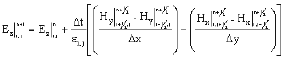 | (5) |
The power transmission spectra are computed by taking the Fast Fourier Transform (FFT) of the fields that are calculated by FDTD and integrating the pointing vector over the cells of the output ports. The computer used in this simulation is P4 3.00 GHz and has 4 GB of RAM.
DESIGN OF NARROW BAND-PASS FILTER STRUCTURE
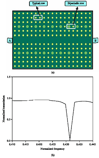
In the first scheme, two cavity-coupled structures are located in both side of an ordinary PC waveguide. This new structure is named biperiodic structure. A typical cavity-coupled waveguide and a biperiodic waveguide are shown in Fig. 1a-b.
First, we consider biperiodic photonic crystal as depicted in Fig. 1c which its structure contains two different lattice constants. In order to have such structure we perturb the period of the two rows next to the waveguide by introducing a new periodicity, a', in these two rows, as shown in Fig. 1c. The new structure is named as the a' structure and regions with periodicity of a is named as the a structure.
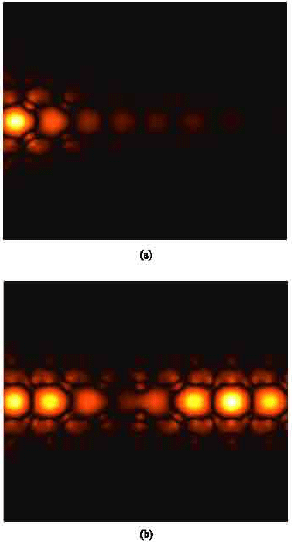
Structures with two, three and nine periods of a' structure are depicted in Fig. 2. These structures act as narrow band-pass filters. It is obvious that transmission amplitude of filter increases by increasing the number of periods in a' structure. Based on our simulations, a biperiodic structure which is shown in Fig. 2e has acceptable normalized transmission. In this structure,normalized transmission is above 98% and fractional bandwidth (Δf/f0) is about 0.005. Two ports of the filter are labeled A and B as shown in Fig. 2a.
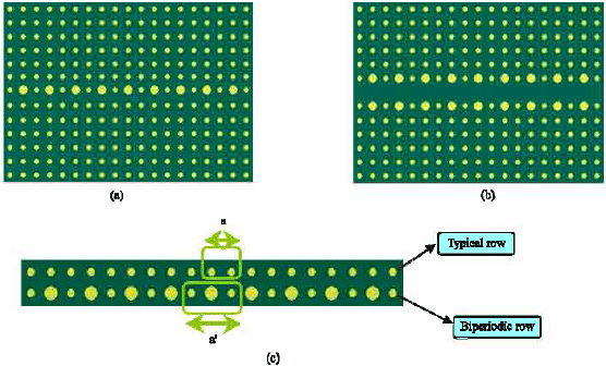 | |
| Fig. 1: | (a) Typical cavity-coupled waveguide, (b) Biperiodic waveguide and (c) Typical and biperiodic rows of photonic crystal |
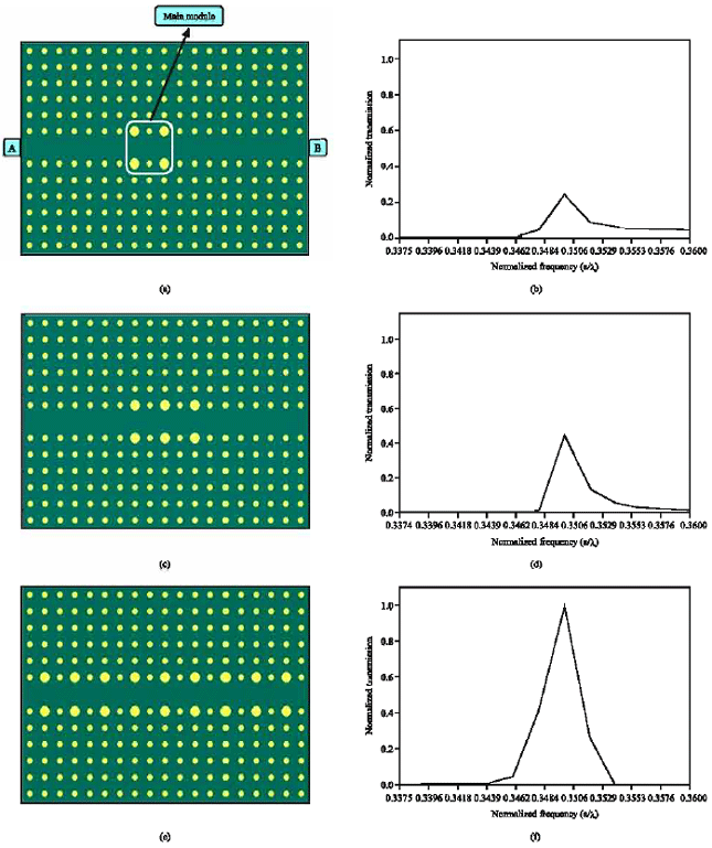 | |
| Fig. 2: | Filter structure with: (a) two periods, (c) three periods and (e) biperiodic photonic crystal; Optical power transmission characteristics of (b) two periods filter, (d) three periods filter and (f) biperiodic filter |
In biperiodic structure, it seems that the main module which is shown in Fig. 2a, acts as super cavity. When this super cavity is put in the waveguide, only frequencies that match super cavities resonant frequency is passed through waveguide while others are reflected. Based on our simulations using array of these super cavities, optimize the output transmission efficiency.
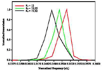 | |
| Fig. 3: | Optical power transmission characteristics of biperiodic structure at: εr1 = 12, F1 = 0.352; εr2 = 12.25, F2 = 0.35; εr3 = 12.5, λ3 = 0.3479 |
The structure used in this section is 2D rectangular lattice of dielectric columns in air host. The dielectric constant of rods is 12.25 and the radii of the rods are 18.5% of the lattice constant. The selected photonic crystal structure has a band gap for TM modes, the band gap associated with this structure varies in the range of normalized frequency, F1 = 0.3103 to F2 = 0.4252 for TMz polarization.
Band-pass filter tunability: One of the most important features of any filter is to be tunable. Here we investigate the effect of changing bigger rod's dielectric constant. This structure is simulated for three different dielectric constants εr = 12, 12.25 and 12.5. The power transmission spectra for these values are depicted in Fig. 3. These dielectric constants lead us to achieve following central normalized frequency of the filter, F1 = 0.352, F2 = 0.35 and F3 = 0.3479, respectively. It is obvious that by raising dielectric constant, central frequency of the filter decreases. Let's think these dielectric rods are made of an electro-optical material so we can change the dielectric constant of the structure. With localized change in dielectric constant of these rods, the central frequency of the filter can be tuned.
The results of time domain simulation after 30000 time step are depicted in the following figure. Figure 4 shows electric field intensity of the band-pass filter at (a) stop normalized frequency of F1 = 0.36 and (b) pass normalized frequency of F2 = 0.352.
 | |
| Fig. 4: | Electric field intensity of band-pass filter at (a) F1 = 0.36 and (b) F2 = 0.352 |
DESIGN OF NARROW BAND-STOP FILTER STRUCTURE
If we increase the distance between a' structure and waveguide, a narrow band-stop filter will be achieved. This is because unlike previous filter that super cavities transfer input signal through output port, in this structure due to distance between a' structure and waveguide, super cavities are destroyed and the bigger rods perform as array of typical cavities with same resonant frequency. These cavities reflect the input signal that match their resonant frequency and allow going out other non resonant frequencies. Quality factor of filter increases as the distance between cavities and waveguide increases (Adibi et al., 2000; Villeneuve et al., 1996). In our simulations, this distance is two lattices constant. In this case a' structure acts as a cavities that reflect the central frequency of the filter as shown in Fig. 5a.
 | |
| Fig. 5: | (a) Filter structure with biperiodic photonic crystal, (b) Optical power transmission characteristics of biperiodic structure |
In similar way, this biperiodic structure has acceptable normalized spectra. In biperiodic structure, normalized transmission is 3% and fractional bandwidth (Δf/f0) is about 0.008 as shown in Fig. 5b. The dielectric constant of the ordinary rods and the bigger rods are 12.25 and 6.6, respectively.
Band-stop filter tunability: Here, we investigate the effect of changing bigger rods' dielectric constant on central frequency of the filter in the new structure. Three different curves are depicted in Fig. 6 for εr = 6.55, 6.6 and 6.65. These dielectric constants lead us to obtain following central normalized frequencies, F1 = 0.4324, F2 = 0.4316 and F3 = 0.4303, respectively. As shown in this figure, central frequency of the filter increases as dielectric constant decreases.
Finally, the results of time domain simulation after 30000 time step are depicted. The Fig. 7 shows electric field intensity of band-stop filter at (a) pass normalized frequency, F1 = 0.425 and (b) stop normalized frequency, F2 = 0.4316.
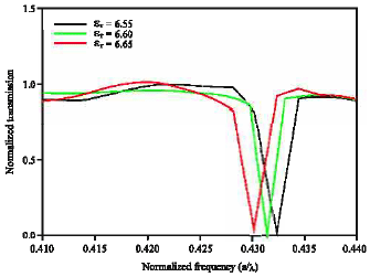 | |
| Fig. 6: | Optical power transmission characteristics of biperiodic photonic crystal at: εr1 = 6.55, F1 = 0.4324; εr2 = 6.6, F2 = 0.4316; εr3 = 6.65, F3 = 0.4303 |
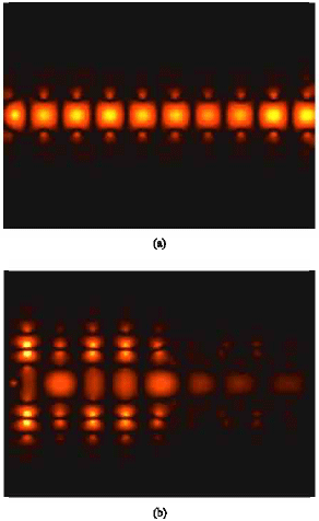 | |
| Fig. 7: | Electric field intensity of band-stop filter at (a) F1 = 0.425 and (b) F2 = 0.4316 |
CREATING DIFFERENT REFRACTIVE INDEXES IN REALITY
We can create the different refractive indexes in reality by using nonlinear material, thermo-optic material, electro-optic material and Selective Modification of Defect's Dielectric Constant method. In nonlinear material, an intense light resonating in one resonant mode can change the refractive index of the resonator. We can use the Thermo-Optic (TO) effect caused by Two-Photon Absorption (TPA) in Si to control the resonator’ refractive index through the heat generated by optically produced carriers. In last method, Figure 8 shows a 2D photonic crystal cavity in which dielectric constant of the cavity has been locally modified.
Several experimental techniques have been developed to locally modify the dielectric constant of semiconductor materials. In the case of III-V semiconductors, Quantum Well Intermixing can be used for this purpose. This method commonly uses a SiO2 layer to promote the out diffusion of Gallium (Ga), creating and diffusing vacancies during a thermal annealing process. This can also be applied to the InP material system with the use of an InGaAs cap on which the SiO2 layer is deposited. The initial steps of fabrication process steps are shown in Fig. 9.
Typical changes in refractive index induced by quantum well intermixing are of about 10%, for example the dielectric constant of the material could be reduced from 11.56 to 11 only (Alvarado-Rodriguez, 2003).
Another alternative to locally changing the dielectric constant of a photonic crystal cavity is to switch to the Silicon-On-Insulator (SOI) material system. Indeed, SOI has recently been used to produce photonic integrated circuits. In SOI, there is a method called Separation by Ion Implantation of Oxygen (SIMOX).
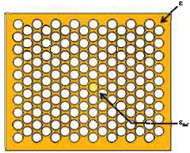 | |
| Fig. 8: | Photonic crystal defect cavity with modified dielectric constant (Alvarado-Rodriguez, 2003) |
In this technique, ions of Oxygen are implanted onto a silicon substrate and SiO2 is formed by thermally annealing. By masking the substrate accordingly, isolated regions of oxide can be formed. Figure 10 depicts the initial process steps followed in SIMOX.
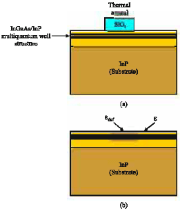 | |
| Fig. 9: | Quantum-Well intermixing process (a) A SiO2 film is patterned on top of an InGaAsP/InP multiple quantum well structure. The wafer is then thermally annealed and (b) The SiO2 film is removed. The dielectric constant of the structure is locally modified (Alvarado-Rodriguez, 2003) |
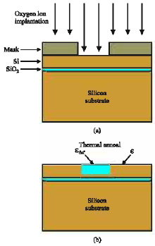 | |
| Fig. 10: | The SIMOX process (a) Oxygen ions are implanted on a masked SOI wafer and (b) The mask is removed and the wafer is thermally annealed. SiO2 is formed in the exposed regions (Alvarado-Rodriguez, 2003) |
For example with this method, it is possible to reduce the dielectric constant from 11.56 to 2.56, closer to what is theoretically required. Furthermore, the use of silicon as a material system can take advantage of the well-developed industry expertise and technology (Alvarado-Rodriguez, 2003).
CONCLUSION
In this study, we proposed new narrow band filters based on biperiodic photonic crystal. Our designed structure have acceptable narrow bandwidth and normalized transmission spectra for the band-pass and band-stop filters are respectively over 98% and below 3% at central frequency of the filters. We discussed about the tunability of these band-pass and band-stop filters, which is achieved by altering the refractive index of bigger rods in biperiodic structure. This leads us to change the central frequency of the filters. Finally, we argued about creating the different refractive indexes in reality.
ACKNOWLEDGMENT
This study was supported by Iran Telecommunication Research Center.
REFERENCES
- Adibi, A., R.K. Lee, Y. Xu, A. Yariv and A. Scherer, 2000. Design of photonic crystal optical waveguides with singlemode propagation in the photonic bandgap. IEEE Elect. Lett., 36: 1376-1378.
Direct Link - Chao, C., X. Li, H. Li, K. Xu, J. Wu and J. Lin, 2007. Bandpass filters based on phase-shifted photonic crystal waveguide gratings. Opt. Express, 15: 11278-11284.
CrossRefDirect Link - Costa, R., A. Melloni and M. Martinelli, 2003. Band-pass resonant filters in photonic-crystal waveguides. IEEE Photonics Technol. Lett., 15: 401-403.
Direct Link - Fan, S., P.R. Villeneuve, J.D. Joannopoulos and H.A. Haus, 1998. Channel drop filters in photonic crystals. Opt. Express, 3: 4-11.
CrossRefDirect Link - Mekis, A., J.C. Chen, I. Kurland, S. Fan, P.R. Villeneuve and J.D. Joannopoulos, 1996. High transmission through sharp bends in photonic crystal waveguides. Phys. Rev. Lett., 77: 3787-3790.
Direct Link - Park, D., S. Kim, I. Park and H. Lim, 2005. Higher order optical resonant filters based on coupled defect resonators in photonic crystals. J. Lightwave Technol., 23: 1923-1928.
Direct Link - Soltani, M., A. Haque, B. Momeni, A. Adibi, Y. Xu and R.K. Lee, 2004. Designing complex optical filters using photonic crystal microcavities. Int. Soc. Opt. Eng., 5000: 257-265.
Direct Link - Villeneuve, P.R., S. Fan and J.D. Joannopoulos, 1996. Microcavities in photonic crystals: Mode symmetry, tunability and coupling efficiency. Phys. Rev. B., 54: 7837-7842.
CrossRefDirect Link