
Musongong, Eugene
Department of Physics, Nasarawa State University, Keffi Nigeria, Nigeria
Journal of Applied Sciences
Year: 2007 | Volume: 7 | Issue: 22 | Page No.: 3391-3399


ABSTRACT
In this study, the variation of electron-lattice temperature in the nanosecond (ns) time regime nearly impossible with metals has been presented and it is clearly shown that non-equilibrium temperature in the nanosecond (ns) time regime of several hundreds of Kelvin temperature of transient hot electrons can be obtained using intrinsic and doped Indium-Antimonide thin film semi-conducting materials. It is shown that Ne(t) versus time profile for different thicknesses of different semi-conducting materials and the exponential growth rate as function of hot electron temperature and time, one can make an approximate estimate of the enhanced electron-concentration. The FWHM of the Te(t) versus time profile is usually around 1 to 4 nanosecond (ns) for film thicknesses of 100 A0 to 1.2 micron though, it increases with film thicknesses. The exponential growth rate varies on the average from 105 to 1010 as electron temperature increases. We noted that the value of the Ne(t)/No (which is the enhancement factor), using t of the order of FWHM is found to vary from 105 to 109. In other words, one can enhance the free electron concentrations in semiconductor conduction band for a time scale of 1 to 4 n sec, using our technique of electron pumping from valence band to conduction band with intense CO2 laser pulse. This is expected to significantly enhance the photo-emission by a suitably delayed probe laser with hv>Φ work function. The delay should be such that the probe laser is switched on after the cessation of the pump laser but within the FWHM period.
PDF Abstract XML References Citation
How to cite this article
Musongong, Eugene, 2007. Enhanced Transient Hot Electron Concentration in n-Type Indium Antimonide (InSb) Semi-Conducting Thin Film in Nanosecond Time Regime. Journal of Applied Sciences, 7: 3391-3399.
DOI: 10.3923/jas.2007.3391.3399
URL: https://scialert.net/abstract/?doi=jas.2007.3391.3399
DOI: 10.3923/jas.2007.3391.3399
URL: https://scialert.net/abstract/?doi=jas.2007.3391.3399
INTRODUCTION
Irradiation of metallic and semi-conducting thin films surfaces with ultra short laser pulses leads to a disturbance of the free-electron gas out of thermal equilibrium. The non-equilibrium dynamics of the electron gas has been an area of intense research both theoretically and experimentally for the past couple of decades (Fujimoto et al., 1984; Jensen et al., 2003). The advent of nanosecond, picosecond and femtosecond laser pulses has greatly enhanced the study of the fundamental processes of electron-electron interaction as well as electron-phonon interaction in these materials (Esarey et al., 1993; James, 1983; Feldstein et al., 1997; Papadogiannis et al., 2001; Rethfeld et al., 2002).
Non-equilibrium between electrons and phonon temperatures (the lattice) in the picosecond and femtosecond time regimes has been very important for metals because it has been widely studied (both theoretically and experimentally) and applied (Fujimoto et al., 1984; Shoenlein, 1996; Shwoerer et al., 2001; Usesaka et al., 2000; Eiguren et al., 2001; Papadogiannis et al., 2001; Rethfeld et al., 2002; Hafz et al., 2003). In a metal however, the free electrons gas first absorbed the energy from the incident laser while the lattice remains cold and transfer the energy to the electrons below through Electron-Electron Collision Time (EECT) (Rethfeld et al., 2002).
After a while, energy is distributed among the free electrons by electron-electron collision leading to the thermalization of the electron gas. A distribution function is assumed to be thermalized depending on the features one wishes to observe. The temperature of the free electron will first rise when there is sufficient non-equilibrium between the electron temperature (Te) and the lattice temperature (Tl) due to the large mass difference between the electrons and phonons; typically, a few tens of picosecond will remain at low temperature (Rethfeld et al., 2002). The process involved with the phenomena mentioned above continued for ultra short laser pulses to a temperature higher by a few thousands of Kevin for a short period of time where local temperature equilibrium is reached. The temperature in this region becomes gradually equal to ambient temperature through relative long procedures in which heat diffusion also plays a key role (Lin and Cheng, 1981; Wu et al., 2001) due energy transfer from electrons to phonons through Electron-Phonon Coupling Time (EPCT). The decoupling is only possible when the free electrons receive energy from the laser at a rate faster than they are able to transfer to the lattice through EPCT coupling. In metal the EPCT is quite strong and that is why it is very difficult to decouple the two temperatures (electron temperature, Te and lattice temperature Tl) when a metal is irradiated by high power laser of nano to pico second pulse width. Conceptually, electron phonon coupling helps the free electron gas assembly to thermally equilibrate (or thermalize) to a single temperature, Te at a given instant of time t, over a time range of Δt; (approximately equal to the collision time) around t, so that the electron energy distribution over a time t + Δt around t can be described on the average by Fermi function with a single temperature as T, with Δt ≤ τ. T is a function of t in these situations and τ is the relaxation time.
The development of photon devices requires the material with both fast optical response speed and large temperature stability (Jensen et al., 2003) provided the damage threshold value of the material is not reached. The semi-conducting thin film of Indium-Antimonide (InSb) becomes an obvious choice since in this paper we have been able to theoretically delay the pulse width and increase the concentration of the charge carrier with a view of obtaining high average non-equilibrium temperature and enhanced free carrier concentration in the conduction band of the material. For a free-electron laser of high brightness, many time repetitions and low emittance, Fujimoto et al. (1984) and others (Jensen et al., 2003) have used tungsten material or metal related materials to obtain non-equilibrium of a few thousand Kelvin. However, the concentration in metal is fixed and can only be irradiated with a femtosecond laser pulses, which hardly yield the above condition for Free-electron laser applications. This idea motives us to theoretically investigate the non-equilibrium system of an intrinsic Indium-Antimonide thin film semi-conducting material by considering the Anisimov et al. (1974) coupled differential equations and applications of appropriate boundary conditions and tailoring the characteristic of semiconductors to our advantage with a view of determining non-equilibrium transient hot electron time profile and the concentration time profile of this material. The focus in this study is therefore geared towards carrying out a theoretical investigation of the possibility of creating very large temperature difference between electrons and lattice (so as to create an appreciable carrier concentration) of semi-conducting thin films of different thickness of material for different pump CO2 laser of different shapes such as Gaussian pulse for time scales of one nanosecond.
THEORETICAL MODEL
When a laser pulse is incident normally on a thin film material, there is an exchange of energy between the electrons and the lattice through electron-phonon interaction governed by a set of coupled nonlinear differential equations given as follows De and Musongong (2007).
We employ Ce and Cl as functions of t(i) and z(j), Ce and Cl are the electronic specific heat capacity per unit volume and lattice specific heat respectively. Kt is the thermal conductivity of the material and g is the electron-phonon coupling. For a thin semi-conducting film of Indium-Antimonide with pump laser incident along the z-direction, the transient electron heating is at z = 0.
| (1) |
Since the lattice receives energy from electrons through electron phonon coupling of both z = 0 and z>0
| | (2) |
is valid.
A (z, t) is the source term which is actually the z-gradient of the incident laser pulse probe intensity and R being the reflectivity at the surface of the material thin film (Indium-Antimonide) at time t. It is natural that there will be a temperature differential due to heating of the material. This has been taken into consideration as the material mounted on a substrate with experimental set up as in De and Musongong (2007). The laser power is assumed to be uniform over the incident surface. Even within the skin depth (δ) of the metal, electrons at different layers receive energy from the laser pulse at different rates because of the
term of the intensity within the metal. The free electrons at a given layer after receiving energy from the laser within Eq. 2. Therefore:
| | (3) |
The boundary conditions that exist at the surface are
| | (4) |
for Gaussian pulse
| | (5) |
Both Te and Tl are functions of and z.
 |
where, NΔz = d
| | (6) |
The electrons at the surface (z = 0) absorb energy from the incident laser pulse through electron phonon coupling. The energy is conducted to electrons in the layers below z = 0 through electronic thermal conductivity. Part of the energy is transferred to the lattice through the term g(Te-Tl) where as the radiation can take place through motion. The electron-phonon coupling factor g is given as:
| | (7) |
where:
| m | = | The effective mass of the electrons or holes. |
| ne | = | The electronic concentration. |
| Vs | = | The velocity of sound in the metal. |
| τep | = | The relaxation time. |
The validity of the two temperatures model (i.e., Te and Tl) is obviously limited to times longer than the electron-electron collision time τee for every material. For this to happen, the metal with suitable femtosecond electron-phonon relaxation time τep becomes an obvious choice suitable since there is strong electron-phonon coupling. We decided to investigate theoretically some of the parameters such as the charge carrier concentration ne that appeared in Eq. 7 as a constant, the transient electron hot temperature (that should be maintained even when the laser source is switched off) and Ce, the electronic specific heat capacity per unit volume of Indium-Antimonide with a view to extending the non-equilibrium to the semi conducting material and in the nanosecond (ns) time regime as an obvious choice. In this study, we considered the electron-phonon coupling g as dynamic rather than a constant as assumed by Fujimoto et al. (1984). Preliminary calculations showed that for semi-conducting thin film, if the concentration of the charge carrier is varied, implies enhancement in the electron-phonon coupling and since τep is given by the expression:
| | (8) |
for semiconductor, while a and b are constants and determined experimentally, photoemission will be enhanced.
ANALYSIS
Thermal enhancement technique, involves laser pumping of electrons from valence band to conduction band and emitting those excited electrons by a delayed laser pulse in addition to those usual photoelectrons from valence band. Here, in order to obtain thermally enhanced photoemission using ultra short laser pulses; time resolved measurement of the electron and lattice temperatures has been studied by James (1983) for some of the semiconductors through impact ionization led exponential growth using CO2 laser. The impact ionization gives an idea of obtaining a non-equilibrium transient hot electron temperature and the lattice temperature using semiconductors. We have decided to employ Eq. 1-7 in our simulations. The idea here is that, if significant temperature difference can be achieved it will lead to enhanced photoemission when using a suitable delayed pulse probe laser. The analytical solution of (1) and (2) along with the boundary conditions is nearly impossible since (1) and (2) are coupled non-linear differential equations. For a given thickness d, relaxation time τ and gradient of the laser intensity A (z,t) we apply numerical finite difference method. We took N = 1000 and further to several thousands, being the divisions of both the time t(i), τ = 1 nanosecond (ns)and the thickness d(j). We took i = 0, 1, 2, 3,…N and j = 0, 1, 2, 3,…N where (i,j) are functions of time and thickness, respectively. We calculated the values of Te (i,j) and Tl(i,j) and obtained the average temperature +Te(i), and +Tl(i),, respectively for intrinsic InSb thin film Fig. 3-9. Here we have assumed
for simplification and better approximation. We took different thicknesses of material with different peak pulses of averagely low intensities.
RESULTS AND DISCUSSION
To apply our method of calculation for enhanced concentration of intrinsic semi-conducting thin film with a variation in the electronic specific heat capacity per unit volume of Indium Antimonide, we apply the derivation specific heat Ce at a temperature Te while adopting the equipartition approach and the quantum approach for the absorption of pulse intensity from the heating CO2 laser. The electron-phonon interactions and absorptions in terms of the Fermi Function f(k) is given in Rethfeld et al. (2002).
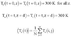
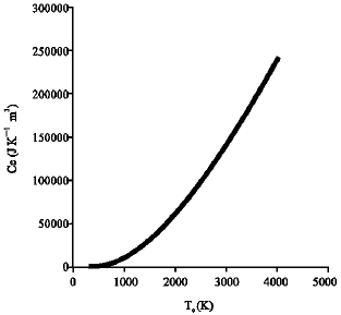
The computed specific heat capacity of the sample is shown in Fig. 1 and 2. Both methods have however shown significant increase in the specific heat capacity when the temperature is increased.
 | |
| Fig. 1: | Temperature dependence of specific heat capacity applying classical approach for InSb |
 | |
| Fig. 2: | Temperature dependence of specific heat capacity applying quantum approach for InSb. |
This idea gives a way of controlling Ce in semiconductors, rather than the constant value assumed by Fujimoto et al. (1984) and Jensen et al. (2003) for metals.
There is a direct relationship of Ce with temperature as it increases progressively and at low temperature the curve seems very sluggish is both cases. This is expected since InSb has a very low value of energy gap εg.
Here Eg is the energy gap, Me*, Mh* are the effective mass of the electron and hole, respectively. Me*, Mh*, εg are given in De and Musongong (2007).
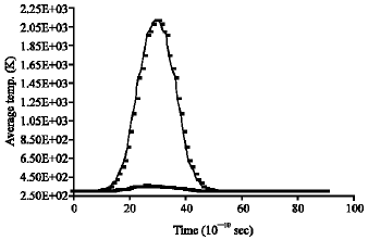
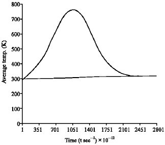
Figure 3-9 show calculations of non-equilibrium electron-lattice temperatures time profile for various values of InSb thin film thicknesses, pulsed laser power and doping concentration. Figure 3 is for doped InSb and Fig. 4-9 is for intrinsic InSb.
 | |
| Fig. 3: | 280 A0 thick of InSb thin film irradiated with 10 MW cm–2 laser pulse with a doped concentration of Nd = 1021 m–3 for Gaussian pulse with τ = 1 n sec |
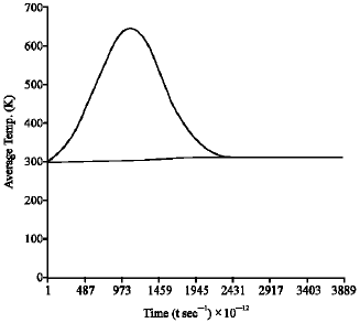 | |
| Fig. 4: | 1.2 μm thick of InSb thin film irradiated with 10–2 MW cm–2 laser pulse with intrinsic concentration for Gaussian pulse |
 | |
| Fig. 5: | 0.9 μm thick of InSb thin film irradiated with 10–2 MW cm–2 laser pulse with intrinsic concentration of for Gaussian pulse |
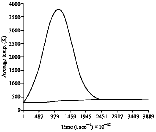 | |
| Fig. 6: | 1.2 μm thick of intrinsic InSb thin film irradiated with 0.1 MW cm–2 laser pulse with a intrinsic concentration for a Gaussian pulse |
For intrinsic InSb the calculations are made using the quantum expression of Ce Fig. 3 shows a 280 A0 thick of InSb thin film irradiated with 108 W m–2 laser pulses. Using Eq. 1-8 and our method of calculating Ce and the electron-phonon coupling, it is seen from Fig. 3-9, that the results obtained here predicts significant non-equilibrium between electron and lattice temperatures in nanosecond time regime. The results showed that <Te(t)>max depends on the thickness of the thin film, the incident laser pulse intensity and the duration of the pulse width.
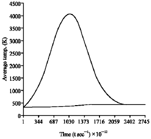 | |
| Fig. 7: | 1.1 μm thick of InSb thin film irradiated with 0.1 MW cm–2 laser pulse with intrinsic concentration of for Gaussian pulse |
 | |
| Fig. 8: | 0.9 μm thick of InSb thin film irradiated with 0.1 MW cm–2 laser pulse with intrinsic concentration of for Gaussian pulse |
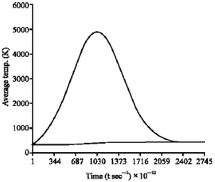
It is worth mentioning here that the result of the quantum derivation of Ce fits well in to the calculations of intrinsic InSb with a significant non-equilibrium electron lattice temperature as obtained in Fig. 4-9. Here, the full wave at half maximum (FWHM) is about 1 nanosecond with a maximum electron temperature ranging from 760 K. to about 5000 K depending on incident laser power intensity and thin film thickness. It could be observed that the transient hot electrons remain significantly hot (in comparison to the lattice temperature) essentially for time scale of the order of 0.5 nanosecond after the cessation of the incident nano-second laser pulse. This feature could be different for other semiconductors such as GaAs, Ge etc. Such differences are expected since the transient electron temperature time profile depends on the electronic properties of the semi-conducting materials that include the effective masses, band gap etc. Figure 9 shows the simulation of +Te(t), for InSb thin films of thickness 0.9, 1.1 and 1.2 μm for a Gaussian pulse peak-power of 0.1 MW cm–2 of the incident laser intensity.
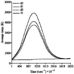 | |
| Fig. 9: | d1 = 1.2 μm, d2 = 1.1 μm, d3 = 0.9 μm thick of InSb thin film irradiated with 0.1 MW cm–2 laser pulse with intrinsic concentration for Gaussian pulse |
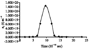 | |
| Fig. 10: | Transient hot concentration-time Ne(t) profile for intrinsic InSb using Te-t in Fig. 9 |
 | |
| Fig. 11: | Exponential growth rate with transient electron temperature of n-type InSb. λ = 9.6 μm |
 | |
| Fig. 12: | Exponential growth rate with transient electron temperature of n-type InSb. λ = 10.6 μm |
 | |
| Fig. 13: | Exponential growth rate with transient electron temperature of p-type InSb. Wavelength λ = 9.6 μm |
The curves depict a transient evolution of non equilibrium electron-lattice temperature of the order, above 3000 K for both thickness of the thin film. The curves show +Te(z,t),max dependent on thickness of film as well as time when the peak power and duration are both held constant. We applied the +Te(z,t),max relations above to calculate the transient hot electron concentration after the cessation of the 1 nanosecond (ns)incident laser as shown in Fig. 10.
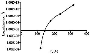
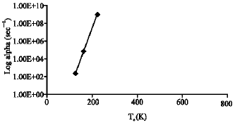
Using the study in James (1983) we proceed to calculate transient hot Concentration-time profile for doped Indium-Antimonide material by first calculating the exponential growth rate as function of transient electron/hole temperatures and subsequent as a function of time. The results of the calculations are shown in the Fig. 11-14.
Figure 11 shows the exponential growth rate verses transient hot electrons temperature irradiated with high intensity CO2 laser of 9.6 μm wavelength of InSb.
 | |
| Fig. 14: | Exponential growth rate with transient electron temperature of p-type InSb. Wavelength λ = 10.6 μm |
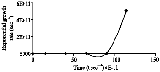 | |
| Fig. 15: | Exponential growth rate as function of time hot electrons in n-type InSb. Wavelength λ = 10.6 μm |
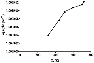
In Fig. 12, n-type InSb is irradiated with 10.6 μm wavelength CO2 laser of high intensity pulse power. It is shown that the gradient of the plot is very stiff due to very short range of temperature. This could be attributed to the chemical properties of the material.
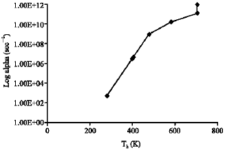
Figure 13 shows the exponential growth rate verses transient hot holes temperature irradiated with high intensity CO2 laser of 9.6 μm wavelength of InSb. The values of the exponential growth rate of hot holes in the semiconductor material are quite high but the transient holes temperature range is short. In Fig. 14, the exponential growth rate verses transient hot holes temperature irradiated with high intensity CO2 laser of 9.6 μm wavelength of the semiconductor material are quite high but the transient temperature range is very short.
In Fig. 15, n-type InSb is irradiated with 10.6 μm wavelength CO2 laser of high intensity pulse power. Here, the exponential growth rate is a function of time. It is shown that the gradient of the plot is very stiff inline with the short range of temperature as shown in Fig. 11-14.
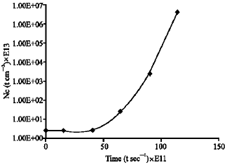 | |
| Fig. 16: | Transient electron concentration-time Ne(t) profile of n-type InSb irradiated with CO2 laser intensity of wavelength λ = 10.6 μm |
Following James (1983) one has calculated the exponential growth rate α(s-1) as a function of Te for various thicknesses of the semiconductors irradiated with laser pulse of different wavelengths, for n-types and p-types (Fig. 11-14) and then based on calculations presented here one has obtained Te(t) profile which then gave us the α(s-1) as a function of time for the CO2 laser pulse irradiation with a given intensity and duration of a semi-conducting thin film of given thickness.
The density of transient hot electron-time profile from impact ionization led exponential growth has been theoretically calculated and presented in Fig. 16. The result shows a gradual increase in the concentration with time as the laser source is heating.
In Fig. 16, n-type InSb is irradiated with 10.6 μm wavelength CO2 laser of high intensity pulse power. It is shown that the concentration gradually built up within the time range of zero to about 0.5 nanosecond before a sudden growth sets in. The plot Ne(t) verses time is shown to terminate at maximum. (i.e., Ne(t) = 1020 m–3). This is not so as the concentration will decay back to the initial concentration as time increases.
Finally our theoretical investigation has shown that semi-conducting film offers an ideal medium of observing non-equilibrium between transient electron temperature and the lattice temperatures in the nanosecond laser pulse time regime. For practical application of these findings, what is important is that one needs to have thin film of proper thickness matching the peak power available laser pulse intensity such that Te stays sufficiently hot (say above 3000 K) over a period three to four times the width of the pump laser pulse, so that a suitably delayed probe laser will be able to photo-emit the hot electrons out of the surface (held at high negative potential with the respect to accelerating anode).
CONCLUSIONS
It is shown that non-equilibrium temperature between Te and Tl can be achieved with InSb semi-conducting thin films both for intrinsic and extrinsic material, which could lead to increase carrier concentration from the concentration verses time profile without affecting the material properties. It is also shown that using our theoretical method formulated for calculating the transient hot carrier concentration in intrinsic InSb semiconducting material and extending that in James (1983) both results agreed perfectly well (Fig. 10 and 16) and is strongly noted here that, among the semiconductors tested with this method only InSb shows significant increase in concentration both using intrinsic and extrinsic material. The experimental set up for this research is found in De and Musongong (2007). It is worth mentioning without reservation that this could lead to enhanced photoemission for Free-electron laser applications and other nano physics technology. The calculation of the true enhancement is another subject of discussion as the process is a two-step multi-photon generation in Milonni and Eberly (1988). When we apply the Richardson-Laue-Dushman expression for the thermionic part, we note the effect is very small. However, this method has increased the substrates list to be used for charge carrier concentration for free electron laser applications for high brightness and low emittance. From what has been presented above on the Ne(t) versus time profile for different thicknesses of different semi-conducting materials and the exponential growth rate as function of hot electron temperature and time, one can make an approximate estimate of the enhanced electron-concentration. This is done as follows: The FWHM (full wave at half maximum) of the Te(t) versus time profile is usually around 1 to 4 nanosecond for film thicknesses of 100 A0 to 1.2 micron though, it increases with film thicknesses (for higher film thicknesses, as seen before higher laser power is required to achieve enhanced electron temperature). The exponential growth rate varies on the average from 105 to 1010 as electron temperature increases. Also, we computed the final concentration Ne(t). We noted that the value of the Ne(t)/No (which is the enhancement factor), using t of the order of FWHM is found to vary from 105 to 109. In other words, one can enhance the free electron concentrations in semiconductor conduction band for a time scale of 1 to 4 nanosecond, using our technique of electron pumping from valence band to conduction band with intense CO2 laser pulse. This is expected to significantly enhance the photo-emission by a suitably delayed probe laser with hv >Φ work function. The delay should be such that the probe laser is switched on after the cessation of the pump laser but within the FWHM period (it is to be noted that as per our calculations the electrons remain significantly hot for time scale of FWHM when the pump laser pulse ceases). It is worth to mention that the thin film semi-conducting materials (because of the peculiar properties of the semiconductors) offer a more reliable lasing action rather than the traditional tungsten metal that has been used Fujimoto et al. (1984) and co workers. This promises to be a prodigious amount of work to be done in the area of solid state physics. The discoveries here are merely a humble beginning of an unlimited wealth of scientific knowledge in the field of laser technology.
REFERENCES
- De, D.K. and E.F. Musongong, 2007. Non-equilibrium electron-lattice heating and enhanced free carrier concentrations in nanosecond CO2 laser pumped semi-conducting GaAs thin film. J. Eng. Applied Sci., 2: 637-647.
Direct Link - Eiguren, A., B. Hellsing, F. Reinert, G. Nicolay and E.V. Chukov et al., 2002. Role of bulk and surface phonons in the decay of metal surface states. Phys. Rev. Lett., 88: 066805-066805.
Direct Link - Esarey, E., S.K. Ride and P. Sprangle, 1993. Nonlinear thomson scattering of intense pulses from beams and plasmas. Phys. Rev. E, 48: 3003-3021.
Direct Link - Feldstein, J.M., C.D. Keating, Y.H. Lian, M.J. Natan and N.F. Scherer, 1997. Electronic relaxation dynamics in coupled metal nanoparticles. J. Am. Chem. Soc., 119: 6638-6647.
Direct Link - Hafz, N., H.J. Lee, T.J.U. Kim, G.H. Kim and H. Suk, 2003. Femosecond X-ray generation via the thomson scattering of a terawatt laser from electron bunches produced from the lwfa utilizing a plasma density transition. IEE Trans. Plasma Sci., 31: 1388-1394.
Direct Link - Rethfeld, B., A. Kaiser, M. Vicanek and G. Simon, 2002. Ultrafast dynamics of nano- equilibrium electrons in metals under femosecond laser irradiation. Phys. Rev. B, 65: 214303-214311.
Direct Link - Schwoerer, H., P. Gibbon, S. Dusterer, R. Behrens and C. Ziener, 2001. Mev X-ray and photo-neutrons from femosecond laser produced plasmas. Phys. Rev. Lett., 86: 2317-2320.
Direct Link - Wu, J.L., Q.F. Zhang, C.M. Wang and Y.H. Zou, 2001. Transient optical relaxation of the cu-bao thin film. Applied Surf. Sci., 183: 80-85.
Direct Link