
Z.A. Zakaria
School of Electrical Engineering, Wuhan University, Wuhan 430072, China
B.C. Chen
School of Electrical Engineering, Wuhan University, Wuhan 430072, China
M.O. Hassan
School of Electrical Engineering, Huazhong University of Science and Technology, Wuhan 430074, China
J.X. Yuan
School of Electrical Engineering, Wuhan University, Wuhan 430072, China
Information Technology Journal
Year: 2008 | Volume: 7 | Issue: 8 | Page No.: 1141-1148


ABSTRACT
This study addresses the transient studies of electrical networks with embedded, distribution static compensator (DSTATCOM) as example of Custom Power (CP) controllers. The transient analysis and modeling is performed with the state-of-the-art digital Simulator PSCAD/EMTDC.4.2. Simulations were carried out for both cases where, DSTATCOM was connected into the system and not, with simulation interval 0.8-1 sec. The aim of the DSTATCOM here to provide voltage regulation at the load point and mitigate the voltage sag generated when the load is increased.
PDF Abstract XML References Citation
How to cite this article
Z.A. Zakaria, B.C. Chen, M.O. Hassan and J.X. Yuan, 2008. Distribution Static Compensator Used as Custom Power Equipment and its Simulation Using PSCAD. Information Technology Journal, 7: 1141-1148.
DOI: 10.3923/itj.2008.1141.1148
URL: https://scialert.net/abstract/?doi=itj.2008.1141.1148
DOI: 10.3923/itj.2008.1141.1148
URL: https://scialert.net/abstract/?doi=itj.2008.1141.1148
INTRODUCTION
An increasing demand for high quality, reliable electrical power and an increasing number of distorting loads have led an increased awareness of power quality both by customers and utilities. For power-quality improvement, the development of power electronic devices such as Flexible AC Transmission System (FACTS) and custom power devices have introduced an emerging branch of technology providing the power system with versatile new control capabilities (Enslin, 1998; Singh et al., 1999). One of the most common power quality problems today is voltage dips which, faced by many industries and utilities. It contributes more than 80% of Power Quality (PQ) problems that exist in power systems (Roger et al., 1996). A voltage dip is a short time (10 msec to 1 min) event during which a reduction in rms voltage magnitude occurs. Faults due to lightning, is one of the most common causes to voltage dips on overhead lines. Among these, the distribution static compensator is most effective devices, based on the VSC principle. A new PWM-based control scheme has been implemented to control the electronic valves in the two-level VSC used in the D-STATCOM.
Custom power is a concept based on the application of power electronic controllers in distribution systems to supply reliable power (Acha et al., 2002; Hingorani, 1995; Taylor et al., 1995; Woodley et al., 1995). Reliability is expanded to include power quality goals: no power interruptions, tight voltage regulation, low harmonic distortion and low phase unbalance (Sabin and Sundaram, 1996). The family of custom power controllers originally included three basic devices (Hingorani, 1995; Taylor et al., 1995): the Solid-State Breaker (SSB), the Static Compensator (DSTATCOM) and the Dynamic Voltage Restorer (DVR). A distribution static compensator is a fast response, solid-state power controller that provides flexible voltage control at the point of connection to the utility distribution feeder for Power Quality (PQ) improvements. It can exchange both active and reactive power with the distribution system by varying the amplitude and phase angle of the converter voltage with respect to the line terminal voltage. A DSTATCOM is also an efficient means for flicker mitigation (Clouston and Gurney, 1999; Larsson and Poumarede, 1999). The interfacing of embedded DC generators, such as fuel cells, with the AC distribution system would require a thyristor-based converter or a VSC (Acha et al., 2002). The VSC connected in shunt with the AC system provides a multifunctional topology which can be used for up to three quite distinct purposes:
| • | Voltage regulation and compensation of reactive power |
| • | Correction of power factor |
| • | Elimination of current harmonics |
Here, such device is employed to provide continuous voltage regulation using an indirectly controlled converter. One of the advantages that this type of compensator has over conventional SVC`s is the improved speed of response. It has been demonstrated that response of a DSTATCOM can change from its full inductive to its full capacitive rating within one cycle. This unprecedented speed of response means that such a device is ideally suited to application with a rapidly varying load (Chen and Ooi, 1999; Clouston and Gurney, 1999; Reed et al., 1999).
The DSTATCOM has plenty of applications in low voltage distribution systems aimed to improve the quality and reliability of the power supplied to the end-user. It can be used to prevent non-linear loads from polluting the rest of the distribution system. The rapid response of the DSTATCOM makes it possible to provide continuous and dynamic control of the power supply including voltage and reactive power compensation, harmonic mitigation and elimination of voltage sags and swells (Acha et al., 2002).
OVERVIEW OF DSTATCOM
Structure of DSTATCOM: Briefly, DSTATCOM structure is based on a simple two-level VSC which is controlled using conventional sinusoidal PWM. Filtering equipment is not included in the design. But, there are several factors that must be considered when designing the DSTATCOM and associated control circuits. In relation to the power circuit the following issues are of major importance:
| • | DC link capacitor size |
| • | Coupling transformer reactance and transformation ratio |
| • | Output filters equipment |
Modelling of DSTATCOM : It is assumed that the source is a balance, sinusoidal three-phase voltage supply with the frequency ω. Since reactive power compensation is desired, it is convenient for this analysis to take the angle of the input the reference angle. However the system is designed based on following assumptions (Schauder and Mehta, 1993):
| • | The three AC mains voltages are balanced |
| • | The three - phase load is balanced and linear |
| • | The inverter switches are ideal |
| • | DC link output is ripple free |
| • | The filter components are reactive and linear |
A DSTATCOM, which is schematically shown in Fig. 1, consists of a two-level Voltage Source Converter (VSC), a DC energy storage device, a coupling transformer connected in shunt to the distribution network through a coupling transformer.
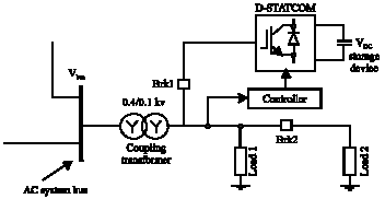 | |
| Fig. 1: | Schematic diagram of test circuit of DSTATCOM to be built in PSCAD |
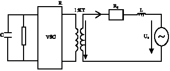 | |
| Fig. 2: | Single-phase equivalent circuit of DSTATCOM |
The VSC converts the DC voltage across the storage device into a set of three-phase AC output voltages. These voltages are in phase and coupled with the AC system through the reactance of the coupling transformer. Suitable adjustment of the phase and magnitude of the DSTATCOM output voltages allows effective control of active and reactive power exchanges between the DSTATCOM and the AC system. Such configuration allows the device to absorb or generate controllable active and reactive power. A single-phase equivalent circuit of DSTATCOM is shown in Fig. 2. Where, Rc is included to represent small losses in the switching devices of VSC. Rs and L represent the equivalent circuit of the tie-transformer between system voltages Us and the output voltage UI of DSTATCOM.
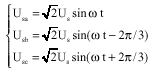
The Usa, Usb, Usc are defined as instantaneous values of system phase voltage and can be given by:
 | (1) |
where, Us is rms value of system phase voltage. The output voltages of DSTATCOM, uja, uib and uic can be given by:
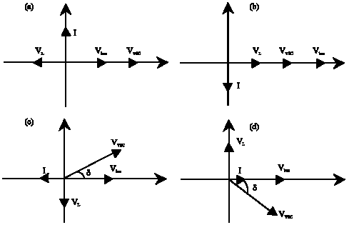 | |
| Fig. 3: | Vector diagram of D-STATCOM (a) Capacitive mode, (b) Inductive mode, (c) Active power release and (d) Active power absorption |
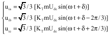 | (2) |
where, KT is turn`s ratio of the tie-transformer, m is the amplitude modulation ratio of VSC output voltage; its value depends on the type of VSC. UDC is the DC-link capacitor`s voltage of VSC and is the phase angle difference between voltage us and ui.
Principle of DSTATCOM: DSTATCOM is to suppress voltage variation and control reactive power in phase with system voltage. It can compensate for inductive and capacitive currents linearly and continuously. Figure 3 shows the vector diagram at the fundamental frequency for capacitive and inductive modes and for the transition states from capacitive to inductive and vice versa. The terminal voltage (Vbus) is equal to the sum of the inverter voltage (VVSC) and the voltage across the coupling transformer reactance VL in both capacitive and inductive modes. I mean that if output voltage of DSTATCOM (VVSC) is in phase with bus terminal voltage (Vbus) and VVSC is greater than Vbus, DSTATCOM provides reactive power to system. And if VVSC is smaller than Vbus, DSTATCOM absorbs reactive power from power system. Vbus and VVSC have the same phase, but actually they have a little phase difference to compensate the loss of transformer winding and inverter switching, so absorbs some real power from system.
Figure 3 is DSTATCOM vector diagrams, which show inverter output voltage VI, system voltage VT, reactive voltage VL and line current I in correlation with magnitude and phase δ. Figure 3a and b explain how VI and VT produce capacitive or inductive power by controlling the magnitude of inverter output voltage VI in phase with each other. Figure 3c and d show DSTATCOM produces or absorbs real power with VI and VT having phase±δ. The transition from inductive to capacitive mode occurs by changing angle δ from zero to a negative value. The active power is transferred from the AC terminal to the DC capacitor and causes the DC link voltage to rise. The active and reactive power may be expressed by the following equations:
| (3) |
| (4) |
SIMULATION OF DSTATCOM
The transient response of any natural system is the way in which the response of the system behaves as a function of time. There are many types of analysis: Steady state, quasi steady state, dynamic and transient. Here, we used transient analysis, by using PSCAD which, is a general purpose time domain simulation tool for examining the transient behaviour of electrical networks. The objectives of the simulation generally include:
| • | Predict the performance of a system |
| • | Identify potential problems |
| • | Evaluate possible problem solutions |
The simulation is especially important for a concept validation and design iteration during a new product development. Here, the DSTATCOM is modelled using the digital simulator PSCAD/EMTDC. Figure 1 shows the schematic diagram of the test system used to carry out the transient modelling and analysis of the DSTATCOM. The test system comprises of a 0.4 kV three-phase transmission system, represented by a Thevenin equivalent feeding into the primary side of a two-winding transformer. A varying load is connected into the 0.1 kV, secondary side of the transformer. A two level VSC-based DSTATCOM is connected to the 0.1 kV to provide instantaneous voltage support at the load point. A 500 μF capacitor on the DC side provides the DSTATCOM energy storage capabilities. Breaker Brk1 is used to control the period of operation of the DSTATCOM and Brk2 controls the connection of load 2 to the system. The aim of the DSTATCOM is to provide voltage regulation at the load point and mitigate the voltage sag generated when the load is increased. The system is considered to be operating under balanced conditions and both loads are linear. The DSTATCOM structure is based on a simple two-level VSC which is controlled using conventional sinusoidal PWM. Filtering equipment is not included in the design.
DSTATCOM controller implemented in PSCAD/ EMTDC, which composed from two parts PWM generators (Fig. 5) and DSTATCOM controller (Fig. 6).
The voltage error signal is obtained by comparing the measured Vrms voltage against a reference voltage, Vrms_ref. The difference between these two signals is processed by a PI controller in order to obtain the phase angle δ required to drive the error to zero. The angle δ is used in the PWM generators as the phase angle of the sinusoidal control signal.
Once the construction of the circuit schematic diagram has been completed (Fig. 4-6 in one PSCAD window), it is run using the module Run Time Executive. Simulations were carried out for both cases, where, DSTATCOM was connected into the system and not. In the simulation interval 0.8-1 sec the load is increased by closing Brk 2. In this same interval Brk.1 is closed and the DSTATCOM stars operating to mitigate the voltage sag and restore the voltage back to reference value. Briefly the following graphic (Fig. 7), explains when the simulations were carried out for both cases, where, DSTATCOM was connected into the system and not with interval 0.8-1 sec.
The set of switches shown in Fig. 4 were used to assist different loading scenarios being simulated with ease. To show the effectiveness of this controller in providing continuous voltage regulation, simulations were carried out with and with no D-STATCOM connected to the system.
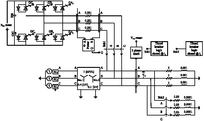 | |
| Fig. 4: | DSTATCOM test system implement in PSCAD/EMTDC |
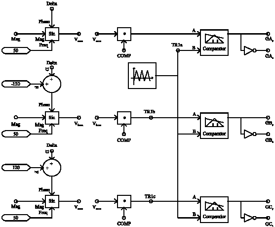 | |
| Fig. 5: | PWM generators impalement in PSCAD/EMTDC |
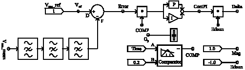 | |
| Fig. 6: | DSTATCOM controller impalement in PSCAD/EMTDC |
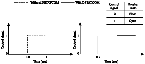 | |
| Fig. 7: | The state of breakers when the simulations were carried out for both cases where, DSTATCOM was connected into the system and not |
SIMULATION RESULTS
Case 1: Simulation results of voltage sag
| • | The first simulation contains no DSTATCOM, in the simulation period 0.8-1 sec; the load is increased by closing switch 2 (Brk2). In this case, the voltage drops by almost 19% with respect to reference value |
| • | The second simulation contains DSTATCOM, under new operating condition (In the same interval Brk.1 is closed) the DSTATCOM starts operating to mitigate the voltage sag and restore the voltage back to reference value, i.e., 1 pu. Fig. 8 shows the voltage Vrms at the load point for both operating conditions |
Case 2: Simulation results of line voltage at the load point
| • | In the first simulation the DSTATCOM is disconnected, during the interval 800-1000 m sec. the result was obtained as Fig. 9a |
| • | The second simulation is carried out using the same scenario as above but now with the DSTATCOM in operation. The simulation clearly shows the capability of the DSTATCOM to mitigate voltage sags providing a continuously variable level of shunt compensation. Figure 9 shows the line voltage Vab at the load point for both operating conditions |
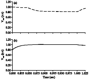 | |
| Fig. 8: | Voltage Vrms at the load point (a) without and (b) with DSTATCOM |
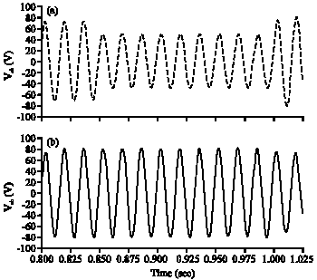 | |
| Fig. 9: | Voltage Vab at the load point (a) without DSTATCOM and (b) with DSTATCOM |
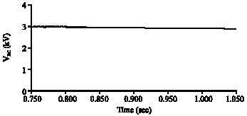 | |
| Fig. 10: | DC voltage when the DSTATCOM is in full operation |
 | |
| Fig. 11: | The reactive power exchange between the AC system and the compensator |
When the DSTATCOM is in full operation, the DC voltage increases to nearly 3 kV (Fig. 10). The reactive power exchange between the AC system and the compensator is shown in Fig. 11.
CONCLUSION AND RECOMMENDATIONS
The use of computer programs in the simulation of Custom Power (CP) controllers (DSTATCOM), including their controls, is extremely important for the development and understanding of this power electronics based technology. The results achieved through the digital simulations clearly show the capability of the DSTATCOM to mitigate voltage sags providing a continuously variable level of shunt compensation of voltage sags and swells.
Hybrid system distribution static compensator (DSTATCOM) with Magnetically Controllable Reactor (MCR) will be required because the advantages of MCR are: simple configuration, less harmonics, relative less response time, larger regulating range, etc. It has not only technical but also economic superiorities and can be widely used to improved the voltage regulation and reactive power compensating of power system, while the distribution static compensator is a fast response, solid-state power controller that provides flexible voltage control at the point of connection to the utility distribution feeder for Power Quality (PQ) improvements, i.e., when the response is fast better use DSTACOM otherwise use MCR.
ACKNOWLEDGMENT
This research was supported by the National Science Foundation of China (Grant No. 50807041).
NOTATIONS
| Us | : | System voltage |
| : | D axis voltage command | |
| UI | : | The output voltage of DSTATCOM |
| : | Q axis voltage command | |
| Usa, Usb, Usc | : | Instantaneous values of system phase voltage |
| : | The DC voltage controller output current command | |
| KT | : | Turn`s ratio of the tie-transformer |
| : | The reactive current command by reactive power controller | |
| Udc | : | The dc-link capacitor`s voltage of VSC |
| δ | : | Firing angle |
| Vbus | : | Bus terminal voltage |
| P | : | Active power |
| VI | : | Inverter output voltage |
| Q | : | Reactive power |
REFERENCES
- Singh, B., K. Al-Haddad and A. Chandra, 1999. A review of active filters for power quality improvement. IEEE Trans. Ind. Electron., 46: 960-971.
CrossRefDirect Link - Schauder, C. and H. Mehta, 1993. Vector analysis and control of advanced static VAR compensators. IEE Proc. C, 40: 299-306.
Direct Link - Chen, Y. and B. Ooi, 1999. STATCOM based on multimodules of multilevel converters under multiple regulation feedback control. IEEE Trans. Power Elect., 14: 959-965.
Direct Link - Taylor, G.A., W.J. Laycock and N. Woodley. 1995. Power quality hardware solutions for distribution systems: CustomPower. Proceedings of the North Eastern Centre Power Section Symposium on the Reliability, Security and Power Quality of Distribution Systems, April 5, 1995, Durham, UK., pp: 11/1-11/9.
Direct Link - Reed, G.F., M. Takcda, I. Iyoda Murakami, T. Aritsuka and K. Tokuhara, 1999. Improved power quality solutions using advanced solid-state switching and static compensation technologies. Proc. IEEE/PES Winter Meeting, 2: 1132-1137.
Direct Link - Enslin, J.R., 1998. Unified approach to power quality mitigation. Proc. IEEE Int. Symp. Ind. Elect. (ISIE ’98), 1: 8-20.
Direct Link - Clouston, J.R. and J.H. Gurney, 1999. Field demonstration of distribution static compensator used to mitigate voltage flicker. Proc. IEEE/PES Winter Meeting, 2: 1138-1141.
Direct Link - Larsson, T.and C. Poumarede, 1999. STATCOM, an efficient means for flicker mitigation. Proceedings of the Power Engineering Society 1999 Winter Meeting, Volume 2, January 31 February 4, 1999, New York, pp: 1208-1213.
Direct Link
arash Reply
hi;
I want to know how did you control D-STATCOM?
and your control is in witch part ?
BR.
Arash.