
G . Josemin Bala
Electronics and Communication Engineering, Anna University, Chennai, India
J. Raja Paul Perinbam
Electronics and Communication Engineering, Anna University, Chennai, India
Information Technology Journal
Year: 2006 | Volume: 5 | Issue: 1 | Page No.: 25-29


ABSTRACT
This study presents a novel architecture for data compression using Adiabatic Logic. The Data Compression unit uses Pass transistor Adiabatic Logic (PAL) Content Addressable Memory (CAM) for pattern matching required by BSTW compression process. SPICE simulation of adiabatic compressor indicate around 50% of power saving at 10 MHZ operating frequency compared to conventional design. Circuits are designed using 0.6 μm CMOS technology.
PDF Abstract XML References
How to cite this article
G . Josemin Bala and J. Raja Paul Perinbam, 2006. A Novel Low Power Adiabatic Data Compressor. Information Technology Journal, 5: 25-29.
DOI: 10.3923/itj.2006.25.29
URL: https://scialert.net/abstract/?doi=itj.2006.25.29
DOI: 10.3923/itj.2006.25.29
URL: https://scialert.net/abstract/?doi=itj.2006.25.29
INTRODUCTION
Data compression is a technique used to increase the effective volume of storage device and the effective bandwidth of data communication channel. Low power and high performance data compressors will play an important role in the growing portable computing and wireless communication markets.
Low power transmission can be achieved by the usage of adiabatic techniques. Adiabatic logic which is also known as energy recovery logic is a new approach to the VLSI circuit design to achieve low power. Adiabatic logic circuits achieve low power dissipation by restricting the current to flow across the device with low voltage drop and by recycling the energy stored on their capacitors[1].
Data compression involves removing the redundancy inherent in information prior to transmission/storage and reinserting it after transmission/access. Several approaches have been proposed for low power data compression . The adaptive data compressor[2] involves selectively shifting the content addressable memory. The CAM based LZ77 data compressor[3] achieves power reduction by shutting off the power for unnecessary comparison between CAM words and input symbol. The LZSS data compressor with dictionary memory of CAM is compared against the incoming string[4]. Power can also be reduced by partial matching data compressor[5]. Compared to all the approaches significant amount of power reduction can be obtained by using adiabatic switching principle.
This research introduces a novel architecture for data compression using Pass transistor Adiabatic Logic (PAL) and compares its power consumption with a LZ data compressor[3].
DATA COMPRESSION
Data compression is based on removing the redundancy from a block of information to result in a equivalent but shorter message. Decompression is the reverse process, namely inserting the redundant information to obtain the original message. Data compression using Huffman coding and Lempel-Ziv coding are quite common compression techniques. They involve lengthy searches of the coding tables and with dynamic implementations, even more complex table manipulation operations. Alternately the BSTW algorithm used for data compression is simpler and support faster compression rates than above coding techniques.
The BSTW algorithm possesses the advantage that it requires only one pass over the data to be transmitted yet has performance which compares well to that of the static two-pass method along the dimension of number of bits per word transmitted. This number of bits is never much larger than the number of bits transmitted by static Huffman coding and can be significantly better. It also incorporates the additional benefit of taking advantage of locality of reference, the tendency for words to occur frequently for short periods of time then fall into long periods of disuse. The algorithm uses a self organizing list as an auxiliary data structure and employs shorter encoding for words near the front of this list. There are many strategies for maintaining self organizing lists. BSTW algorithm uses move-to-front.
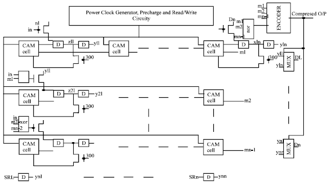 | |
| Fig. 1: | Proposed data compressor architecture |
OPERATION OF BSTW ALGORITHM
A table of N records is held. Data of size m bits (tuple) is compared against each entry in the table. The table is maintained as an N length move to front list.
If the source data matches any entry in the table, an n bit code associated with that tuple is transmitted. The tuple is placed at the top of the list. Since n<m less bits are transmitted. If the source data cannot find a match in the table, the tuple is sent together with an n bit code representing the symbol for the source. Assuming that the incoming data is in the table, more often than not, data compression occurs.
Since bits are used to represent the source, there comes a point when all codes are used. In this case a new tuple needs to be allocated a code currently given to another tuple.
The reallocation algorithm works as follows: The oldest entry is deleted from the bottom of the list. Allocate the code to the new data item. The new entry is inserted at the top of the list. Decoding involves maintaining a similarly structure table at the receiving end. The advantage of this algorithm is that it that is dynamic, yet the table is self-organizing through the simple move to front approach.
ARCHITECTURE
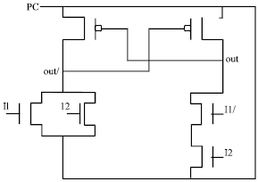
The proposed architecture is based on Content Addressable Memory(CAM) array. A CAM is a circuit element which can be read/written like an ordinary memory. In addition it can compare its stored data with an externally supplied search argument and indicate whether it matches or mismatches.
The architecture of the proposed compression unit is shown in Fig. 1. The move to front strategy necessitates a reorganization of the data in table. The matching word must be identified, then the data in the array above the matching word must all be shifted down one position, resulting in the overwriting of the matching word. The third and final operation is the writing of the input word into the first entry in the table. When there is no matching word, all table entries are shifted down one place, and the new input data written into the first entry in the table. Shifting the data to its neighbour below is carried by the addition of D-latches.
Data enters the system and is latched. This value is then compared with all the entries in the table simultaneously. The matching word address is encoded from the response of the CAM word and output. In addition, it is also fed back into the combinational logic book, which determines which words are to be shifted. Following the shift, the input data is written into the first entry of the table.
ADIABATIC DESIGNS
Pass transistor Adiabatic Logic (PAL)[6,7] is a dual rail logic with true and complementary functional blocks and cross coupled PMOS latch.
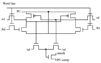 | |
| Fig. 2: | PAL CAM cell |
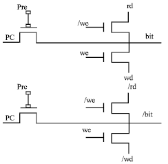 | |
| Fig. 3: | Precharge and read/write circuitry |
A sinusoidal Power Clock (PC) supplies the PAL. The Power Clock for the proposed adiabatic data compressor architecture is generated using the dual rail resonant clock driver circuit[8].
CAM STRUCTURE
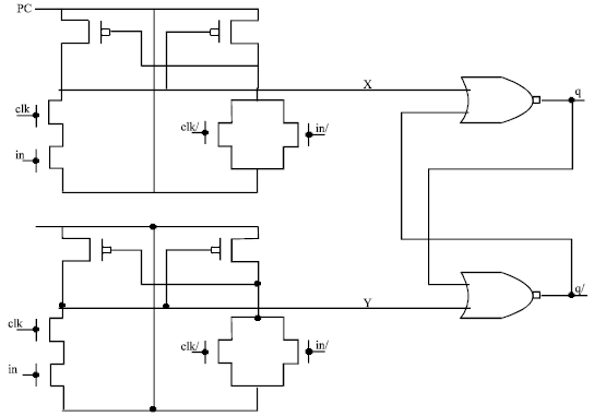
The Fig. 2 shows the PAL CAM cell. The dual lines (bit and bit/) are precharged by the PC to recover the energy before the read operations. Separate data lines are used for writing and reading the data. It has separate precharge and read write circuitry (Fig. 3). The write enable (we) line decides the operation whether to read or write.
In the compare operation, the match line is pre-discharged initially. When a mismatch occurs, the transistor connected to match line is ON and the match line follows PCcomp, Thereby maintaining a very low potential drop across the match line capacitance.
The PCcomp is less than PC since swing in the match line is maintained to a value of one threshold voltage less than the full rail, to decrease the charge loss that would arise across the transistor. The charging and discharging path are the same for the match line and the charge stored is recovered in the same cycle. The match line is therefore held low after the evaluation phase, because the energy is recovered by ramping down the power clock.
MULTIPLEXER AND ENCODER
The PAL multiplexer and a PAL encoder are used in the proposed architecture(Fig. 4 and 5).
When PC starts rising from low, input states make a conduction path from the PC through one of the functional blocks to the corresponding output node and allow it to follow the PC. The other node will be tri-state and kept close to 0 V by its load capacitance. This in turn causes one of the PMOS transistors to conduct and charge the node that should go to one state, up to the peak of PC. The output state is valid at around the top of the PC. The PC will then ramp down towards zero, recovering the energy stored on the output node capacitance.
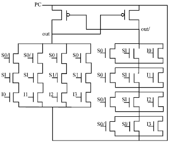 | |
| Fig. 4: | 4x1 PAL multiplexer |
 | |
| Fig. 5: | 2x1 PAL encoder |
 | |
| Fig. 6: | PAL D Latch |
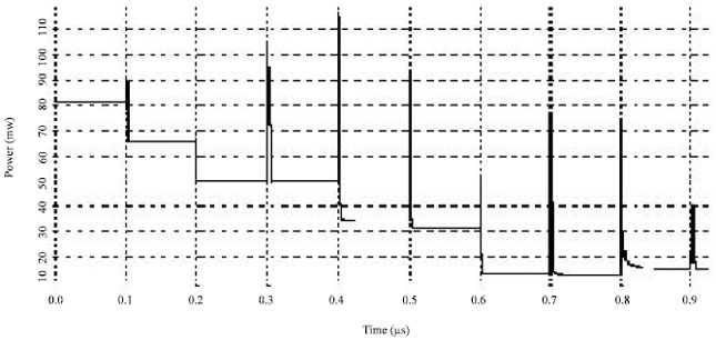 | |
| Fig. 7: | Power consumption of non-adiabatic compressor |
D LATCH
The Fig. 6 shows the design of D Latch used in the proposed architecture. The data input changes in accordance with the clocking time. When the rising edge of PC arrives, the cross coupled PMOS devices sense and latch the appropriate value of the clocked D onto the nodes X and Y. Since the cross coupled NOR gates form a simple set/reset latch, the positive pulses on either X or Y will cause the latch to either set or rest, respectively. When D is not changing, either X or Y will remain low, with the other node oscillating in phase with PC in an energy recovering manner, that is, transferring charge to/from the PC signal.
RESULTS AND DISCUSSION
From the generalised architecture we developed a compression hardware of 4-entry table with 4 bits entries using 0.6 μm CMOS technology.
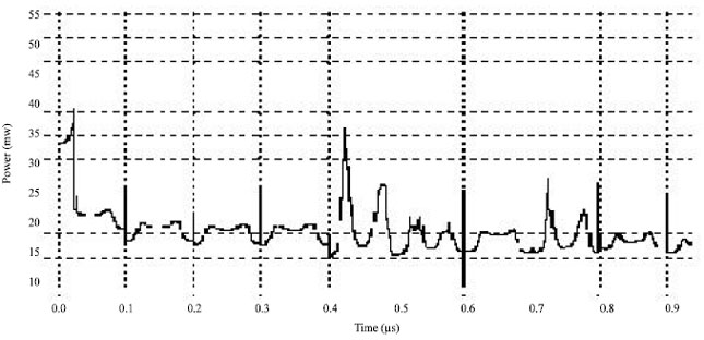 | |
| Fig. 8: | Power consumption of adiabatic compressor |
This provided compression of around 50%. Each primary output was connected to a 50 fF load. To compare the performance adiabatic data compressor, we also developed non-adiabatic data compressor [3].The SPICE simulations computed the overall power dissipation of both the circuits.
The Fig. 7 and 8 shows the power consumption of non-adiabatic compressor and adiabatic compressor. Though the number of transistors is more in the case of adiabatic compressor its average power consumption is 40 mw whereas for non-adiabatic compressor it is 110 mw. Thus simulation results of adiabatic design indicate around 50% of power savings at 10 MHz operating frequency with 5 V PC compared to the non-adiabatic design.
The adiabatic circuits have efficiently charged the capacitors and recycled the energy instead of wasting energy by heating the transistors. Although the proposed PAL compressor has more transistors, the simulation results shows significant power savings at operating frequencies on the order of few MHZ. The results also shows that the Pass transistor adiabatic logic is well suited for designing low power systems with memories.
REFERENCES
- Athas, W.C., L.J. Svensson, J.G. Koller, N. Tzartzanis and E.Y. Chou, 1994. Low power digital systems based on adiabatic switching principles. IEEE Trans. VLSI Syst., 2: 398-407.
Direct Link - Jones, S., 1992. 100 Mbit/s adaptive data compressor design using selectively shiftable content-addressable memory. IEEE Proc. Part G, Circuits Devices Syst., 139: 498-502.
Direct Link - Lin, K.J. and C.W. Wu, 2000. A Low power CAM design for LZ data compression. IEEE Trans. Comput., 49: 1139-1145.
Direct Link - Belle, W., Y. Wei, R. Tarver, J.S. Kim and N.G. Kevin, 1993. A single chip lempel-ziv data compressor. Proceedings of the IEEE International Symposium on Circuits and Systems, May 3-6, Chicago, IL., USA., pp: 1953-1955.
CrossRef - Jones, S., 2000. Partial-matching lossless data compression hardware. IEEE Proc. Comput. Digital Techniques, 147: 329-334.
Direct Link - Oklobdzija, V.G., D. Maksimovic and F. Lin, 1997. Pass-transistor adiabatic logic using single power-clock supply. IEEE Trans. Circuits Syst. II: Analog Digital Signal Process., 44: 842-846.
CrossRefDirect Link - Meimand, H.M., A.A. Kusha and M. Nourani, 2000. Efficiency of Adiabatic logic for low-power, low-noise VLSI. Proceedings of the 43rd IEEE Midwest Symposium on Circuits and Systems, 2000, Lansing, MI., USA., pp: 324-327.
CrossRef - Athas, W.C., N. Tzartzanis, L.J. Svensson and L. Peterson, 1997. A low-power microprocessor based on resonant energy. IEEE J. Solid-State Circuits, 32: 1693-1700.
Direct Link