
A. N. Abdalla
Faculty of Electrical and Electronic Engineering, University Malaysia Pahang, Pekan26600, Malaysia
Ruzlaini Ghoni
Faculty of Electrical Automation Engineering Technology, TATiUC24000, Terengganu, Malaysia
N. F. Zakaria
Faculty of Electrical and Electronic Engineering, University Malaysia Pahang, Pekan26600, Malaysia
Journal of Applied Sciences
Year: 2011 | Volume: 11 | Issue: 5 | Page No.: 768-777


ABSTRACT
Matrix converters as induction motor drivers have received considerable attention in recent years because of its good alternative to Voltage Source Inverter Pulse Width Modulation (VSI-PWM) converters. This study focus on developing a mathematical model for a Space Vector Modulated (SVM) direct controlled matrix converter. The mathematical expressions relating the input and output of the three phase matrix converter are implemented by using MATLAB/SIMULINK. The duty cycles of the switches are modeled using space vector modulation for 0.5 and 0.866 voltage transfer ratios. Simulations of the matrix converter loaded by passive RL load and active induction motor are performed. A unique feature of the proposed model is that it requires very less computation time and less memory compared to the power circuit realized by using actual switches. In addition, it offers better spectral performances, full control of the input power factor, fully utilization of input voltages, improve modulation performance and output voltage close to sinusoidal.
PDF Abstract XML References Citation
Received: October 06, 2010;
Accepted: December 13, 2010;
Published: February 24, 2011
How to cite this article
A. N. Abdalla, Ruzlaini Ghoni and N. F. Zakaria, 2011. Simulation Model of Space Vector Modulated Control Matrix Converter-fed Induction Motor. Journal of Applied Sciences, 11: 768-777.
DOI: 10.3923/jas.2011.768.777
URL: https://scialert.net/abstract/?doi=jas.2011.768.777
DOI: 10.3923/jas.2011.768.777
URL: https://scialert.net/abstract/?doi=jas.2011.768.777
INTRODUCTION
Recently, the induction motor fed from three phase matrix converter has established their importance in industrial drive applications. In reality, the matrix converter provides important benefits such as bidirectional power flow, sinusoidal input current with adjustable displacement angle (i.e., controllable input power factor), and a great potential for size reduction due to the lack of dc-link capacitors for energy storage (Alesina and Venturini, 1989; Casadei et al., 2002; Wheeler et al., 2002).
Various modulation methods for matrix converters have been investigated. Indirect AC-AC modulation (Hara et al., 2004), PWM patterns for nine switches of the matrix converter are generated directly from the output voltage reference and the input current reference. In virtual AC-DC-AC modulation (Itoh et al., 2004), the matrix converter is controlled as a combination of a virtual current source PWM rectifier and a virtual voltage source PWM inverter, and then switching patterns for the matrix converter are synthesized. In the latter case, the problem is that when switching patterns are generated to obtain a zero voltage vector in the virtual inverter, phase currents do not flow in the virtual rectifier regardless of the switching patterns for the rectifier, and as a result, the input current waveforms become distorted. In this problem was solved by changing the carrier wave on the virtual inverter side (Itoh et al., 2004). Another solution involves applying space vector modulation to the virtual rectifier inverter control (Cha and Enjeti, 2003; Helle et al., 2004; Huber and Borojevic, 1995). In another method, the maximum input line-to-line voltage is discarded in PWM modulation when the modulation factor is low, thus suppressing harmonics in the output voltage (Odaka et al., 2009). The present study deals with Space Vector Modulation (SVM) in virtual rectifier inverter control within the frame-work of virtual AC-DC-AC modulation.
In this study, induction motor fed by direct controlled matrix converter with a Space Vector Modulated (SVM) was proposed. A complete mathematical analysis of the power circuit along with the duty cycle calculation (switching algorithm) is described for both low voltage transfer ratio (0.5) and maximum voltage transfer ratio (0.866). The whole model is then realized by using Simulink blocks such as math operators, relational operators, and delay circuits. Finally, the proposed mathematical model is validated using a passive RL load and active induction motor load.
SPACE VECTOR MODULATION
Space Vector Modulation refers to a special switching sequence which is based on the upper switches of a three phase matrix converter. Theoretically, SVM treats a sinusoidal voltage as a phasor or amplitude vector which rotates at a constant angular frequency, ω. This amplitude vector is represented in d-q plane where it denotes the real and imaginary axes. As SVM treats all three modulating signals or voltages as one single unit, the vector summation of three modulating signals or voltages are known as the reference voltage, Voref which is related to the magnitude of output voltage of the switching topologies. The aim of SVM is to approximate the reference voltage vector, Voref from the switching topologies.
For a balanced three phase sinusoidal system the instantaneous voltages may be expressed as (1)
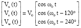 | (1) |
This can be analyzed in terms of complex space vector:
| (2) |
where ejθ = cos + j sinθ and represents a phase shift operator and 2/3 is a scaling factor equal to the ratio between the magnitude of the output line-to-line voltage and that of output voltage vector. The angular velocity of the vector is ω0 and its magnitude V0.
Similarly, the space vector representation of the three phase input voltage is given by (3)
| (3) |
where Vi is the amplitude and ωi, is the constant input angular velocity.
If a balanced three phase load is connected to the output terminals of the converter, the space vector forms of the three phase output and input currents are given by:
| (4) |
| (5) |
Respectively, where ![]() is the lagging phase angle of the output current to the output voltage and
is the lagging phase angle of the output current to the output voltage and ![]() is that of the input current to the input voltage.
is that of the input current to the input voltage.
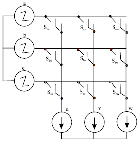 | |
| Fig. 1: | Three phase matrix converter |
Switching principle: The three phase matrix converter (MC) topology is shown in Fig. 1.
Since MC connects load directly to the voltage source by using nine bidirectional switches, the input phases must never be shorted, and due to the inductive nature of the load, the output phases must not be left open. If the switching function of a switch, Sij in Fig. 1, is defined as :
| (6) |
The constraints can be expressed as:
| (7) |
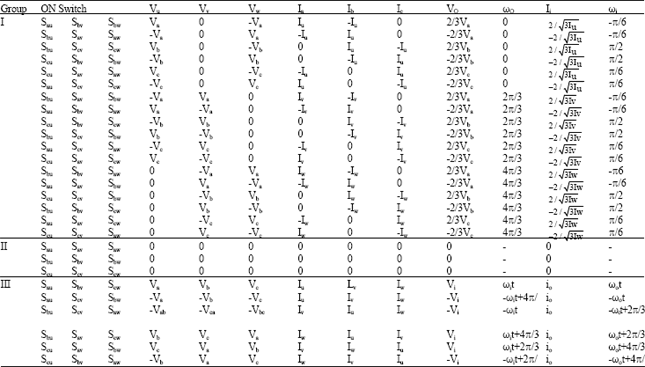
For a three phase MC there are 27 valid switch combinations giving thus 27 voltage vectors as shown in Table 1. The switching combinations can be classified into three groups which are, synchronously rotating vectors, stationary vectors and zero vectors.
CONTROL ALGORITHM
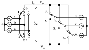
The indirect transfer function approach is employed in both voltage source rectifier (VSR) and voltage source inverter (VSI) parts of the MC. Consider the VSR part of the circuit in Fig. 2 as a standalone VSR loaded by a dc current generator, idc.
Voltage source rectifier space vector modulation: The VSR input current vector diagram is shown in Fig. 3. The space vector of the desired input current can be approximated by two adjacent as shown in Figure 4.
| Table 1: | Matrix converter switching vectors |
 | |
 | |
| Fig. 2: | Indirect matrix conversion |
 | |
| Fig. 3: | Input current vector diagram |
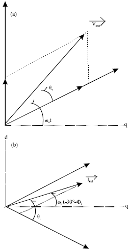 | |
| Fig. 4: | Vector diagrams (a) output sextant 2 (b) input sextant 1 |
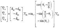
The duty cycles for VSR are calculated as (8)-(10).
| (8) |
| (9) |
| (10) |
where mi is the VSR modulation index:
| (11) |
For a switching cycle within the first sector:
 | (12) |
Substitute θi with:
| (13) |
φi is the arbitrary angle. The transfer matrix of the VSR, ![]() is defined as:
is defined as:
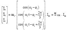 | (14) |
Replacing the modulation index from (11) in (14) resulting the desired input current phase. The VSR output voltage is determined as:
| (15) |
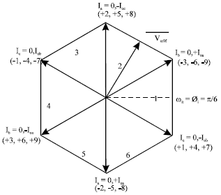
Voltage space inverter space vector modulation: Consider the VSI part of the MC in Fig. 2 as a standalone VSI supplied by a dc voltage source Vpn=Vdc. The VSI switches can assume only six allowed combinations which yield nonzero output voltages.
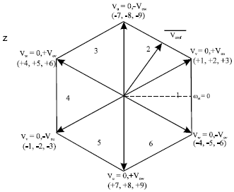 | |
| Fig. 5: | Output voltage vector diagram |
Hence, the resulting output line voltage space vector is defined by Eq. 2 can assume only seven discrete values, V0 – V6 in Fig. 5, known as voltage switching state vectors.
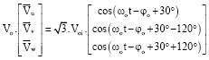
The space vector of the desired output line voltages is
| (16) |
can be approximated by two adjacent state vectors Vd and Vq, and the zero voltage vector, Vo using PWM as shown in Fig. 4, where ![]() is the sampled value of
is the sampled value of ![]() at an instant within the switching cycle Tg. The duty cycles of the switching state vectors are;
at an instant within the switching cycle Tg. The duty cycles of the switching state vectors are;
| (17) |
| (18) |
| (19) |
where, mv is the VSI modulation index
| (20) |
The sectors of the VSI voltage vector diagram in Figure 5 correspond directly to the six sextants of the three phase output line voltages shown in Fig. 6.
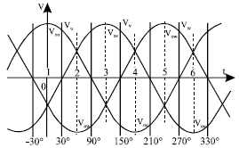 | |
| Fig. 6: | Six sextants of the output line voltage waveforms |
The averaged output line voltages are:
 | (21) |
For the first sextant,
and,
| (22) |
By substitution of (22) in (21):
 | (23) |
Substituting the modulation index from (20) in (23), the output line voltages are obtained:
 | (24) |
The VSI averaged input current is determined as:
| (25) |
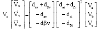
Output voltage and input current SVM: Direct converter modulation can be derived from the indirect transfer function. First modulation is carried out as if the converter is an indirect. The switch control signals for DMC are then derived based on the relation between the VSR and VSI. The modulation index of the DMC is given as:
| (26) |
For simplicity, mv=1 and m=mi.The modulation algorithm is derived similar to VSR and VSI except in the opposite direction. Since, both the VSR and VSI hexagons contain six sextants; there are 36 combinations or operating modes. However, only 27 valid switch combinations giving thus 27 voltage vectors as shown in Table 1. If the first output voltage and the first input current are active, the transfer matrix become:
 | (27) |
The output line voltages are:
 | (28) |
| (29) |
which finally yield to:
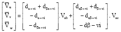 | (30) |
Where,
 | (31) |
As can be seen, the output line voltages are synthesized inside each switching cycle from samples of two input line voltages, Vab and Vac.
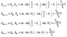
By comparison of (30) and (31), it can be concluded that simultaneous output voltage and input current SVM can be obtained by employing the standard VSI SVM sequentially in two VSI sub topologies of the three phase MC.
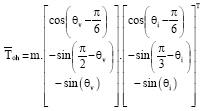
When the standard VSI SVM is applied in the first VSI sub topology, where Vpn=Vab, the duty cycles of the two adjacent voltage switching state vectors are da-vi and dβα-vi as defined in (31). The standard VSI SVM in the second sub topology, with Vpn=Vac, results in the state switching vector duty cycles dαβ-vi and dβ-vi, also defined as (31). The remaining part of the switching cycle is given as:
| (32) |
MATHEMATICAL MODELING
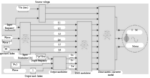
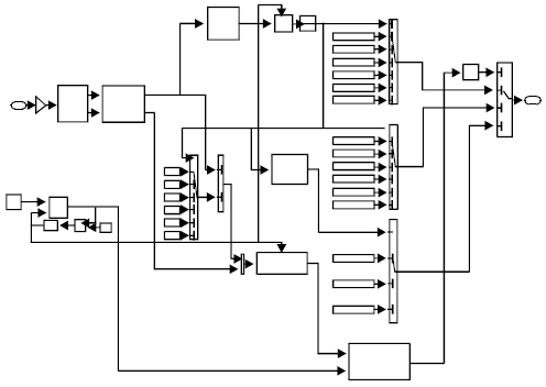
The complete model of MC is shown in Fig. 7. It comprises input modulator, output modulator, MC modulator and MC IGBTs switches.
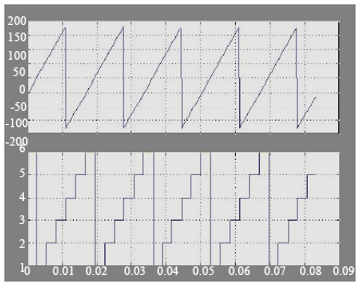
Figure 8 is the sector identification and reference angle generation. The angle is generated from the reference output frequency by integrating it. Based on the angle, the sector can be identified. The result is shown in Fig. 11. The modulation of input current is shown in Fig. 9; the output voltage modulation is similar to VSI. The switch control signals for MC are shown in Fig. 10.
RESULT AND DISCUSSION
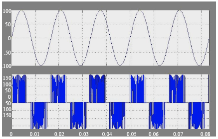
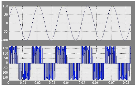
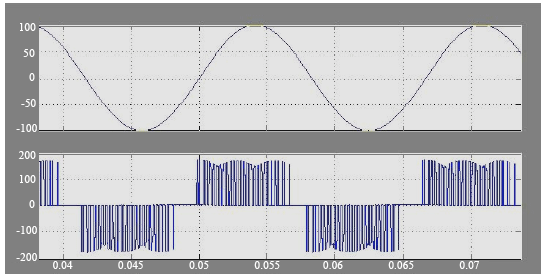
The simulations of direct matrix converter are carried out using MATLAB/SIMULINK. The processing took 56 sec for the passive RL load and 45 sec for the induction machine load. It was loaded by three phase induction motor (3 hp, 200 V, 60 Hz star connected) for 0.5 and 0.866 transfer ratio.
Figure 11 shows the sector identification and reference angle generation. The angle is generated from the reference output frequency by integrating it. Based on the angle, the sector can be identified.
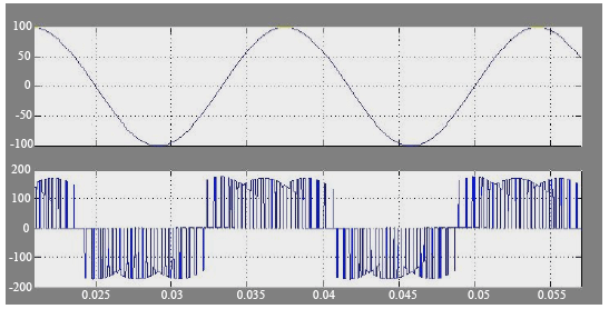
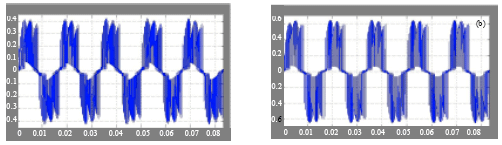
The input and output line voltage with loaded passive load is shown in Fig. 13 and 14 for transfer ratio of 0.5 and 0.866. For the induction machine loaded the simulation result is shown in Fig. 15 and 16. Figure 16 and 17 is the input current for the passive load and induction motor load respectively. The input currents are mostly sinusoidal for the induction motor load.
 | |
| Fig. 7: | Block diagram of simulation model for direct matrix converter |
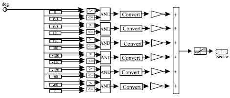 | |
| Fig. 8: | Sector identification |
 | |
| Fig. 9: | Input modulation |
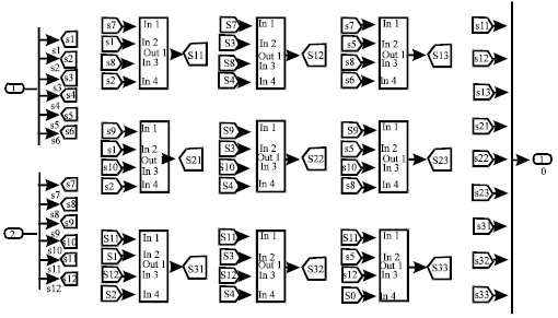 | |
| Fig. 10: | Direct matrix converter modulator |
 | |
| Fig. 11: | Result for sector identification |
 | |
| Fig. 12: | Input and output voltage with passive load for q=0.5; R=135.95Ω, L=168.15 mH, Vim=100 V, fo = 60 Hz, fs = 2 kHz |
 | |
| Fig. 13: | Input and output voltage with passive load for q=0.866; R=135.95Ω, L=168.15 mH, Vim=100 V, fo = 60 Hz, fs = 2 kHz |
 | |
| Fig. 14: | Input and output voltage with loaded induction motor for q=0.5; 3 hp, Rs =0.277Ω, Rr=0.183Ω, Nr=1766.9 rpm, Lm=0.0538H, Lr=0.05606H, Ls=0.0533H, fo=60 Hz, fs=2 kHz |
 | |
| Fig. 15: | Input and output voltage with loaded induction motor for q=0.866; 3 hp, Rs =0.277Ω, Rr=0.183Ω, Nr=1766.9 rpm, Lm=0.0538H, Lr=0.05606H, Ls=0.0533H, fo=60 Hz, fs=2 kHz |
 | |
| Fig. 16: | Input current with passive load; R=135.95Ω, L=168.15 mH, Vim=100 V, fo = 60 Hz, fs = 2 kHz (a) q=0.5, (b) q = 0.866 |
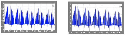 | |
| Fig. 17: | Input current with loaded induction motor for q=0.866; 3 hp, Rs =0.277Ω, Rr=0.183Ω, Nr=1766.9 rpm, Lm=0.0538 H, Lr=0.05606H, Ls=0.0533 H, fo=60 Hz, fs=2 kHz |
CONCLUSION
The main constraint in the theoretical study of matrix converter control is the computation time it takes for the simulation. This constraint has been overcome by the mathematical model that resembles the operation of power conversion stage of matrix converter. This makes the future research on matrix converter easy and prosperous. The operation of direct control matrix converter was analysed using mathematical model with induction motor load for 0.866 voltage transfer ratio.
ACKNOWLEDGMENT
The authors thank the Faculty of Electrical and Electronic Engineering of WHO that funded the project with resources received for research from both University of Malaysia Pahang and TATi University College (Short Grant 9001-9001).
REFERENCES
- Alesina, A. and M.G.B. Venturini, 1989. Analysis and design of optimum-amplitude nine-switch direct AC-AC converters. IEEE Trans. Power Electron., 4: 101-112.
CrossRef - Wheeler, P.W., J. Rodriguez, J.C. Clare, L. Empringham and A. Weinstein, 2002. Matrix converters: A technology review. IEEE Trans. Ind. Electron., 49: 276-288.
CrossRef - Itoh, J.I., I. Sato, H. Ohguchi, K. Sato, A. Odaka and N. Eguchi, 2004. A control method for matrix converter based on virtual Ac/Dc/Ac conversion using carrier comparison method. Trans. Ind. Appl., 124: 457-463.
CrossRef - Cha, H.J. and P.N. Enjeti, 2003. An approach to reduce common mode voltage in matrix converter. IEEE Trans Ind. Appl., 39: 1151-1159.
CrossRef - Helle, L, K.B. Larsen, A.H. Jorgensen, S. Munk-Nielsen and F. Blaabjerg, 2004. Evaluation of modulation schemes for three-phase matrix converters. IEEE Trans. Ind. Electron, 51: 158-171.
CrossRef - Huber, L. and D. Borojevic, 1995. Space vector modulated three-phase to three-phase matrix converter with input power factor correction. IEEE Trans. Ind. Applic., 31: 1234-1246.
CrossRef - Odaka, A., I. Sato, H. Ohguchi, Y. Tamai, H. Mine and J.I. Itoh, 2009. A PAM control method for a matrix converter based on a virtual AC/DC/AC conversion method. Electrical Eng. Japan, 166: 88-96.
CrossRef - Casadei, D., G. Serra, A. Tani and L. Zarri, 2002. Matrix converter modulation strategies: A new general approach based on space-vector representation of the switch state. IEEE Trans. Ind. Electron., 49: 370-381.
CrossRef
arash firoozi Reply
hello
i need your simulation ( Space Vector Modulated Control Matrix Converter-fed)
pleas send for me
thanks
pouria mohtasham Reply
I need the simulation ,too-I will be grateful if you mail it to me:-)
Nguyen Gia Hoang Anh Reply
hi!Now, I am reseaching this subject, I need your simulation please send for me, Thank so much.
Zachary Reply
Hi,
I am also doing research in this subject but I just started and I need your simulation.
Thanks,
Zachary
C.RAJESHKUMAR Reply
Hi Sir, I am C.RAJESHKUAMR., ME(power electronics student) for my final year project i would like to do your topic with fuzzy control,so i need your simulation for my reference sir,,So please send me if you are willing to provide me.
thank you sir,
best regards,
C.RAJESHKUMAR
manoj Reply
hello i need your simulation ( Space Vector Modulated Control Matrix Converter-fed) pleas send for me thanks