
Mamun B.I. Reaz
Department of Electrical, Electronic and Systems Engineering, Universiti Kebangsaan Malaysia, 43600 UKM, Bangi, Selangor, Malaysia
Weng F. Lee
Emerald Systems Design Center, Jalan Sultan Azlan Shah, 11900 Penang, Malaysia
Nor H. Hamid
Universiti Teknologi Petronas, Bandar Seri Iskandar, 31750 Tronoh, Perak, Malaysia
Hai H. Lo
Universiti Teknologi Petronas, Bandar Seri Iskandar, 31750 Tronoh, Perak, Malaysia
Ali Y.M. Shakaff
Universiti Malaysia Perlis, Kampus Kubang Gajah, 02600 Arau, Perlis, Malaysia
Journal of Applied Sciences
Year: 2009 | Volume: 9 | Issue: 14 | Page No.: 2613-2618


ABSTRACT
This study describes an efficient design methodology from an industrial perspective on utilizing Register Transfer Level (RTL) coding style, full scan chain implementation and Automatic Test Pattern Generation (ATPG) to achieve a high percentage of testability in the final Integrated Circuit (IC). The design methodology involves using an ASIC design flow with scan insertion and scan stitching performed after synthesis with scan flops set as don’t_use during synthesis process. Based on this method of ASIC design flow with the RTL coding style and guideline, an in-house 64 bit processor core that executes 3 instructions per cycle, is implemented with 0.35 micron process technology with a single scan chain of 4600 flip-flops, achieving an ATPG pattern for stuck-at at 100% test coverage and 99.81% fault coverage. Thus, creating high testability coverage with the ATPG pattern can be achieved by having a fully synchronous design using the proposed RTL coding style and full scan chain implementation. This study also describes the work around methods used when dealing with cost reduction involving reduction of test pin on the IC chip package.
PDF Abstract XML References Citation
How to cite this article
Mamun B.I. Reaz, Weng F. Lee, Nor H. Hamid, Hai H. Lo and Ali Y.M. Shakaff, 2009. High Degree of Testability Using Full Scan Chain and ATPG-An Industrial Perspective. Journal of Applied Sciences, 9: 2613-2618.
DOI: 10.3923/jas.2009.2613.2618
URL: https://scialert.net/abstract/?doi=jas.2009.2613.2618
DOI: 10.3923/jas.2009.2613.2618
URL: https://scialert.net/abstract/?doi=jas.2009.2613.2618
INTRODUCTION
A common method to implement Design for Test (DFT) into a commercial design is using scan chain and ATPG (Mentor Graphics Corporation, 2006; Lee, 2007). Scan chain and ATPG is commonly used for commercial design as it is a highly automated process providing very good test coverage for a high quality IC chip. Apart from full scan chain and ATPG, there are many other methods of DFT implementation in commercial design such as Built-In-Self-Test (BIST) (Cheah et al., 2003; Lee et al., 2003), Memory BIST (MBIST) (Mentor Graphics Corporation, 2006; Cooley, 2000), JTAG (Joint Test Action Group) (Paddock, 1999), boundary scan (Mentor Graphics Corporation, 2006) and Logic BIST (LBIST) (Apte, 2003). Each of these DFT methods is targeted for different type of DFT testing. For example, memory BIST is targeted for built-in-self-test for memory components within the IC chip, LBIST is targeted for built-in-self-test for logic components and JTAG and boundary scan is targeted to test circuit boards after manufacturing.
Scan chain and ATPG is the most common implementation for DFT as has clear advantages such as (Mentor Graphics Corporation, 2006):
| • | Highly automated process whereby the scan insertion, scan stitching and ATPG pattern generation requiring very little manual effort |
| • | It is a highly effective, well understood and accepted method for generating high test coverage |
| • | It assures good quality on the manufactured part as the circuit can be tested thoroughly during manufacturing using the ATPG pattern |
Scan chain can be divided into full scan and partial scan (Mentor Graphics Corporation, 2006; Lee, 2003, 2007; Mentor Graphics Corporation, MBIST, 2006). Whether it is a full or partial scan, the objective is to modify the sequential elements in the design to behave as easily testable combinational logic. This is done by replacing the sequential elements of a design with a scan flip-flop (a scan flip-flop is a multiplexed flip-flop), as shown in Fig. 1 .
In full scan chain implementation, every single flip-flop is replaced by an equivalent scan flip-flop. Each of those scan flops are stitched together to form a scan chain with a TI (test input) pin, TO (test output) pin, TE (test enable) pin and TCLK (test clock pin, commonly shared with the clock pin of the IC chip).
In partial scan chain implementation, only a portion of the flip-flops in the design is replaced by an equivalent scan flip-flop, which are then stitched together to form a scan chain. This method is sometimes implemented instead of full scan chain due to certain portion of the design being asynchronous and thus not scanable, or due to limited silicon area or performance constraint.
Upon implementation of scan chain, ATPG can generate a set of test patterns that can be used to test for defects on the IC chip. Therefore it is important to ensure that a design can achieve a full scan chain and a high percentage of coverage can be achieved through the ATPG pattern, which will ease the testing for defects on the IC chip. This can be achieved by following a fully synchronous design through proper design methodology and RTL coding guideline as discussed in this study.
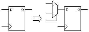 | |
| Fig. 1: | Replacement with scan flops |
MATERIALS AND METHODS
Figure 2 shows a design methodology used for ASIC design (Lee, 2003, 2007, 2000) with a full scan implementation. During synthesis, constraints are used to drive the synthesis such as timing requirements, rise/fall requirements, load requirements and wireload models. Apart from these, DFT constraint of set_dont_use <mux_flop_name> or set_dont_use <scan_flop_name> is used to ensure synthesis does not use any scan flip-flops or multiplexed flip-flops when building the logic circuits. This ensures the synthesized circuit consist only D flip-flops that can be easily replaced by multiplexed flip-flops or scan flip-flops during the scan insertion phase of the design flow.
When synthesis have completed, the scan insertion phase occurs whereby D flip-flops are replaced by multiplexed flip-flops or scan flip-flops which are then stitched together during scan stitching. In this phase, all the multiplexed flip-flops or scan flip-flops are stitched to form a chain starting with TI pin to TO pin as shown in Fig. 3.
With this flop replacement, timing of the circuit will have changed and timing paths that earlier passed setup and hold time requirements during synthesis may fail now due to the additional delay caused by the multiplexer in the multiplexed flip-flop or scan flip-flop. Static timing analysis performed after scan stitching will catch these failures due to the additional delay caused by the multiplexer.
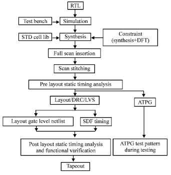 | |
| Fig. 2: | Design methodology for ASIC design |
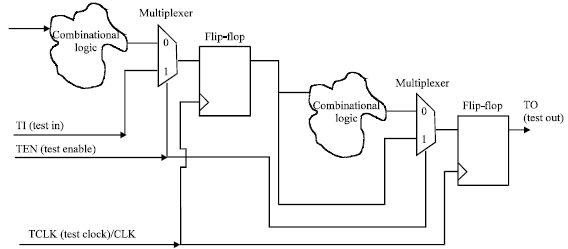 | |
| Fig. 3: | Stitching of scan cells from TI to TO |
RULES DURING RTL CODING AND SYNTHESIS
To ensure high testability, a design have to be fully synchronous and certain RTL guidelines must be followed in order to ensure proper scan chain implementation allowing for good ATPG pattern coverage. The following rules during RTL coding stage and synthesis stage must be followed in order to achieve a fully synchronous design that is scan chain and ATPG friendly (Mentor Graphics Corporation, 2006, Lee, 2000, 2003, 2007, Mentor Graphics Corporation, MBIST, 2006; Mentor Graphics Corporation, LBIST, 2006):
| • | RTL code is separated between sequential elements and combinational elements |
| • | Only flop based sequential elements are allowed. Latch based design is avoided. Having latches in a design not only complicates scan chain development but also complicates static timing analysis |
| • | The clock inputs of the flip-flops are considered golden and not driven by any combinational logic. Clock buffering is only done in clock tree synthesis stage of auto-place-route layout |
| • | Delay cells are avoided in RTL coding stage. Any required delay cells is inserted during failures of static timing analysis |
| • | For large hierarchical design, the output of each module stage is flopped to end the path at the output stage of the corresponding module |
| • | Avoid any combinational feedback loops as these circuits have inherent testability problems (Mentor Graphics Corporation, 2006; Lee, 2007) |
| • | Any parts of the design module that is not scannable needs to be clearly identified and specified during the scan chain insertion to avoid it being included in the scan chain and thus complicating the scan chain |
By adhering to these rules during RTL coding stage, a high degree of design synchronous is achieved, thus providing the design to have a high degree of testability.
ATPG TEST COVERAGE
Using the RTL coding rules mentioned in the previous section and the ASIC design flow of Fig. 2 , a fully synchronous design of an in-house 64 bit processor core that executes 3 instructions per cycle, is implemented with 0.35 μ process technology with a total gate count of approximately 400 k transistors, with a total of 4600 flip-flops. All the sequential flip-flops are replaced with scan flops for a full scan chain implementation and stitched together to form one single scan chain. The ATPG using stuck-at algorithm generated an ATPG pattern with 100% test coverage and 99.81% fault coverage, giving a high coverage (In ATPG pattern generation, the ATPG tool Mentor Graphics’ Fastscan calculates the test coverage and fault coverage based on the patterns achieved using the conditions specified in the Mentor Graphics Fastscan user reference).
The generated ATPG pattern is used during testing of the IC chip to compare the expected results of ATPG with the output of the IC chip as shown in Fig. 4. If the pattern matches with the IC chip output, then the IC chip is clean from any faults. If there are mismatches between the outputs of the IC chip with the expected patterns of ATPG, there are faults in the IC chip.
For large designs that have a heavy depth on the scan chain, it may be considered to use more than one scan chain. For example, by using two scan chain, the depth per chain is reduced by half and thus reducing the ATPG pattern depth. However, having more than one scan chain have its disadvantages:
| • | Increasing testing cost as the tester needs to address more than one scan chain |
| • | Tester load board need to have more than one set of scan in and scan out ports |
| • | Amount of chips that can be tested in parallel using the same tester is reduced as tester needs to drive more pins per chip |
Whether to use more than one scan chain depends on the balancing of cost between costs saved from reduced ATPG pattern depth to additional cost due to the disadvantages.
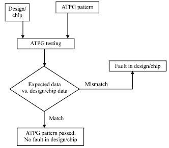 | |
| Fig. 4: | Comparing ATPG test pattern |
SHARING SCAN PINS WITH FUNCTIONAL PINS
Having scan chain and ATPG for testing of IC chips requires four additional pins, namely TI, TO, TCLK, TEN or sometimes also referred to as scan_in, scan_out, scan_clk and scan_enable, for one scan chain (Mentor Graphics Corporation, 2006; Mentor Graphics Corporation MBIST, 2006, Lee, 2003, 2000). If a chip has two scan chains running in parallel, this translates to six additional pins of scan_in1, scan_in2, scan_out1, scan_out2, scan_clk, scan_enable. The more pins on a package translates to higher costs. To avoid this situation, one method used for implementing scan chain and ATPG is by sharing the scan_in pins with input functional pins, scan_out pins with output functional pins, scan_clk with functional clock pin. This leaves only one additional pin required which is the scan_enable pin.
To further reduce cost by removing the scan_enable pin, an internal register can be created as a scan_enable register which defaults to a value of 0. If a write of 1 occurs to this register, it will put the chip into a scan mode. Basically the Q output of the scan_enable register acts as an internal scan_enable signal putting the chip into a scan mode as shown in Fig. 5. The decoding logic to decode a write of 1 to the scan_register and the scan_register itself is excluded from the scan chain and therefore will not be part of the ATPG testing pattern. As a result, if a defect occurs in the decoding logic or the scan_register, the ATPG testing pattern will not be able to catch the fault.
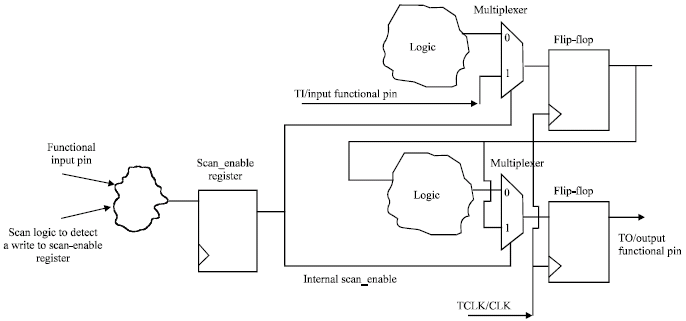 | |
| Fig. 5: | Sharing scan pins with functional pins |
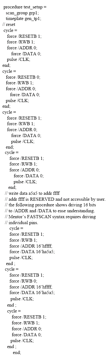
For such design that uses an internal scan register to determine whether the chip is in scan mode, additional test procedures needs to be specified to the ATPG tools during the ATPG test pattern generation. Using Mentor Graphics as an example for generating ATPG test pattern, the following test procedure can be used to specify to the Mentor Graphics Fastscan that additional pattern is needed in order for the chip to enter scan mode.
 |
CONCLUSION
A high degree of design synchronous is achieved, thus providing a high degree of manufacturability and testability. For designs that have a deep depth of flip-flops, more than one scan chain can be used to reduce the depth of the ATPG pattern. A further cost reduction on chip level testing can be achieved by sharing the scan pins (TI, TO, TCLK) with normal functionality pins, with the exception of TE. An internal scan enable register can be written with a pre-assigned address and data that is internally decoded and set the internal scan enable register to a scan enable mode, thus putting the chip in scan mode.
ACKNOWLEDGMENT
The authors would like to express sincere gratitude to the Emerald Systems Design Center, Jalan Sultan Azlan Shah, 11900 Penang, Malaysia for their continuous help and support to materialize this research.